


US Unveils Vision for $3 Billion National Advanced Packaging Manufacturing Program to Bolster Semiconductor Industry
CHIPS for America unveiled its USD 3 billion vision for the National Advanced Packaging Manufacturing Program. Which will be used for the development of an advanced packaging piloting facility for validating and transitioning new technologies to US manufacturers. The first funding for materials and substrates will be unveiled in 2024.
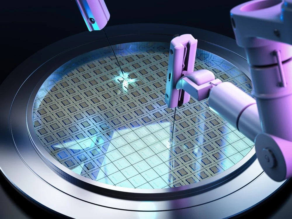
“Advanced Packaging” refers to many microchips with different functionalities assembled tightly together on a substrate at extremely fine dimensions. Developing these advanced packaging capabilities in the US is crucial for driving the country’s technological leadership and economic security. The CHIPS for America R&D program will support the development of advanced packaging technology in the US.
Find out the latest SemiconductorGet Started Now!
Fab Projects in the United States.
CHIPS Research and Development Director Lora Weiss stated that The National Advanced Packaging Manufacturing Program will be collaborating with all CHIPS for America's R&D programs like the National Semiconductor Technology Center. Laurie E Locasio director of NIST stated that within a decade America will manufacture and package the world's most sophisticated chips.
The NAPMP will build and foster a thriving advanced packaging ecosystem by:
- Establishing an advanced packaging and piloting facility that facilitates the adoption of innovations in packaging, equipment, and process development to manufacturing.
- Development of digital tools to enhance efficiency
- cultivating and sustaining collaborations
The six priority research investment areas of NAPMP are:
- Material and Substrates
- Equipment, tools, and processes
- Chiplet ecosystem
- Co-design of multi-chipset systems with automated tools
- Photonics and connectors that communicate with the outside world.
About Chips for America Initiative

The CHIPS for America initiative is a comprehensive effort by the United States government to strengthen the semiconductor industry in the United States. The initiative includes a USD 52 billion investment in semiconductor manufacturing, research and development, and workforce training. The goal of the initiative is to increase U.S. semiconductor production, reduce reliance on foreign suppliers, and strengthen the U.S. economy and national security. Some of the notable projects funded by the CHIPS for America initiative include:
- Intel's new fabs in Arizona: Intel is investing $20 billion to build two new fabs in Chandler, Arizona. The fabs are expected to be operational in 2024 and will produce leading-edge chips. Intel's new fabs in Arizona
- TSMC's new fabs in Phoenix: TSMC, one of the world's largest semiconductor manufacturing companies, is investing USD 40 billion to build two new fabs in Phoenix, Arizona. The fabs are expected to be operational in 2024 and 2026 and will produce advanced and mature-node semiconductors.
- Micron's new fab in New York: Micron is investing USD 100 billion to build a "megafab" in Clay, New York. The fab is expected to be completed in phases over 20 years, with the first phase being operational in 2023. The fab will produce DRAM and NAND flash memory.
- Samsung's new fab in Texas: Samsung is investing USD 17 billion to build a new fab in Taylor, Texas. The fab is expected to be operational in 2024 and will produce leading-edge chips.
Find Upcoming and Ongoing Semiconductor Fabrication Plant Projects in the United States with Ease.
Are you looking for a platform that gives you reliable, high-quality, and timely project insights for Semiconductor Manufacturing Projects in the United States?
Discover the Global Project Tracking (GPT) platform by Blackridge Research, designed to provide you with the most recent United States Semiconductor Fabrication Plant Projects and Tenders better and faster across various stages of development:
- Upcoming projects
- Tender Notices
- Contract award announcements
- Projects in progress or under construction
- Successfully completed projects.
The user-friendly interface helps you obtain early-stage awareness of projects and find the right business opportunity quickly.
Each project will have all the essential details, such as scope, capacity, CapEx, status, project description, companies involved, funding information, location, periodic updates, important event dates like construction start date, commissioning dates, and key contact information of project owners and stakeholders.
The database is a vital resource for a wide range of entities, including semiconductor manufacturers, EPC Companies, silicon material suppliers, data analytics and software providers, consulting and advisory firms, investors, multilateral banks and financial institutions, and law firms.
Book a Free demo to learn more about the United States Semiconductor Fab Projects and Tenders database and how we can help you achieve your goals.
Leave a Comment
We love hearing from our readers and value your feedback. If you have any questions or comments about our content, feel free to leave a comment below.
We read every comment and do our best to respond to them all.