


Taylor Semiconductor Manufacturing Plant Becomes Samsung Electronics' Largest Investment in USA
|
|
|
|
|
|
Project at a Glance
|
|
| |
|
|
|
|
|
|
Project Name
|
|
Taylor Semiconductor Manufacturing Plant
|
|
|
|
|
|
|
|
Project Type
|
|
Greenfield
|
|
|
|
|
|
|
|
Project Location
|
|
Taylor, Texas, USA
|
|
|
|
|
|
|
|
Sector
|
|
Construction
|
|
|
|
|
|
|
|
Subsector
|
|
Semiconductor Plant
|
|
|
|
|
|
|
|
Project Value
|
|
USD 25 billion
|
|
|
|
|
|
|
|
Project Status
|
|
Under Construction
|
|
|
|
|
|
|
|
Main Contractors
|
|
Yates Construction and Samsung C&T
|
|
|
|
|
|
|
|
Project Developer/Coordinator
|
|
Samsung Electronics
|
|
|
|
|
|
|
|
Project Start Date
|
|
2022
|
|
|
|
|
|
|
|
Project Completion Date
|
|
July 2026
|
|
|
|
|
|
|
|
Special Mention
|
|
The largest-ever investment by Samsung in the US
|
|
|
|
|
|
|
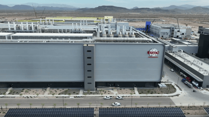
Project Overview
Taylor Semiconductor Manufacturing Plant is the largest-ever investment made by Samsung Electronics in the United States. The groundbreaking ceremony of this project was held in 2022, and the operations are said to begin in July 2026.
The total estimated cost for the project is USD 25 billion, according to officials. Samsung Electronics has chosen Yates Construction and Samsung C&T as the general contractors for the Taylor Semiconductor Manufacturing Plant.
Project Background
Samsung Electronics, one of the largest semiconductor manufacturers in the world announced its plan to to build a semiconductor wafer fabrication plant in Taylor, Texas in November 2021. This decision was made by Samsung in the midst of a global scarcity of chips, which has had a negative impact on numerous industries, including the automotive and electronics sectors.
According to the company's statement, it will continue to help clients all over the world by making advanced semiconductor fabrication more accessible and by satisfying the growing need for semiconductor products.
Samsung's decision to set up this plant in the USA can also be attributed to the CHIPS Act (Creating Helpful Incentives to Produce Semiconductors and Science Act). It is a federal law in the United States that intends to enhance domestic semiconductor manufacturing and research endeavors. As per the Act, the US government has allocated USD 52.7 billion over a five-year period to bolster research, development, and manufacturing initiatives in the semiconductor sector.
Trusted by Leading Manufacturers & EPCs
Find The Latest Semiconductor Fabrication Plant Projects In The United States
Gain exclusive access to our industry-leading database of Semiconductor Fabrication Plant Projects opportunities with detailed project timelines & stakeholder information.
No credit card Up-to-date coverage
Taylor Semiconductor Manufacturing Plant Location Details
Samsung's Semiconductor Manufacturing Plant is strategically located in Taylor, a city in Texas. Samsung's current facility in Austin is just 25 km southwest of Taylor which is one of the reasons for the selection of this location for the manufacturing plant.
Multiple locations were viewed by the company and finally, the investment in Taylor was based on its multifaceted benefits such as the local semiconductor ecosystem, support of local government, stability in infrastructure, and opportunities for community development.
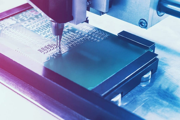
Project scope
Samsung Electronics together with Yates Construction and Samsung C&T are constructing the technologically advanced semiconductor facility in Taylor, Texas. The construction work started in the first half of 2022 and included a building for the supply of chemicals and gases, an office building, a massive back house, a water reclamation facility, and a substation for electricity.
To mitigate the impact of surface tremors, both the production plant and the primary offices have been suspended using drilled shafts anchored into the ground. A total of 20,000 holes were drilled, accommodating piers extending 110 feet into the ground for stabilization. Notably, the project incorporates specialized exhaust ducts with a diameter of 14 feet. The construction process was expedited through the widespread utilization of precast concrete in the facility.
The plant also includes an air separation plant to produce gases such as liquid nitrogen and argon. The company also plans to install electrolyzers for the supply of hydrogen. The new 4 nm designs that Samsung has developed will be used by the Taylor semiconductor plant to manufacture chips. This project is expected to generate 2,000 direct jobs.
The project is spread over an area of 1,200 acres and is the largest-ever investment made by Samsung Electronics in the United States. Making use of cutting-edge process technologies, the new facility will produce goods that can be utilized in a variety of fields, including mobile, fifth-generation (5G) wireless networks, artificial intelligence (AI), and high-performance computing (HPC).
Taylor Semiconductor Manufacturing Plant Project Cost
When the project was announced, the estimated cost of construction was set at USD 17 billion out of which USD 6 billion was to be spent on buildings and other property improvements and USD 11 billion on machinery and equipment. However, the budget was revised to USD 25 billion.
Samsung is looking for a solid public partner to help with the project, offering monetary assistance as well as other benefits including utilities and infrastructural support. As this project falls under the purview of the Chips Act, it will receive aid worth up to 15% of the total cost from the federal government of the United States.
Trusted by Leading Manufacturers & EPCs
Find The Latest Semiconductor Fabrication Plant Projects Around The World
Gain exclusive access to our industry-leading database of Semiconductor Fabrication Plant Projects opportunities with detailed project timelines & stakeholder information
No credit card Up-to-date coverage
Contractors Involved
Samsung Electronics has chosen Yates Construction and Samsung C&T as the general contractor for the project. An agreement was signed between Samsung and EPCOR Utilities Inc. to build a water pipeline from Alcoa to the plant.
The other contractors involved in the gab project in the USA include Samsung E&C America, Samsung Engineering, Austin Bridge & Road, Blue Sky, Coreslab Structures (Texas), Heldenfels Enterprise, Hensel Phelps, JMEG, and Lauren Concrete.
Conclusion
The Taylor Semiconductor Manufacturing Plant project will result in the construction of a technologically advanced facility that is geared toward producing sophisticated semiconductor products. Through the promotion of innovation and the fulfillment of the ever-growing need for semiconductor components, this enterprise intends to make a substantial contribution to the technological landscape.
Taylor's dedication to achieving perfection in both the production and innovation of semiconductors is aligned with the completion of this project. It will mark an important turning point in the expansion of commercial capabilities.
Find Upcoming and Ongoing Semiconductor Fabrication Plant Projects in the USA with Ease.
Are you looking for a platform that gives you reliable, high-quality, and timely project insights for Semiconductor Manufacturing Projects in the USA?
Discover the Global Project Tracking (GPT) platform by Blackridge Research, designed to provide you with the most recent USA Fabrication Plant Projects and Tenders better and faster across various stages of development:
Upcoming projects
Tender Notices
Contract award announcements
Projects in progress or under construction
Successfully completed projects.
The user-friendly interface helps you obtain early-stage awareness of projects and find the right business opportunity quickly.
Each project will have all the essential details, such as scope, capacity, CapEx, status, project description, companies involved, funding information, location, periodic updates, important event dates like construction start date, commissioning dates, and key contact information of project owners and stakeholders.
The database is a vital resource for a wide range of entities, including semiconductor manufacturers, EPC Companies, silicon material suppliers, data analytics and software providers, consulting and advisory firms, investors, multilateral banks and financial institutions, and law firms.
Book a Free demo to learn more about the USA Semiconductor Fab Projects and Tenders database and how we can help you achieve your goals.
Leave a Comment
We love hearing from our readers and value your feedback. If you have any questions or comments about our content, feel free to leave a comment below.
We read every comment and do our best to respond to them all.