


Samsung Electronics plans to invest around USD 280 million to build an advanced chip packaging research facility in Japan. Japan’s industry ministry stated that it would provide Samsung subsidies worth up to USD 140 million.
In March, it was reported that Samsung was seeking to establish a packaging facility in Kanagawa Prefecture. Where the company already has a research and development center.
Find Semiconductor Projects and tenders in JapanGet Started Now!
Samsung will be able to strengthen its semiconductor leadership and form strategic alliances with Yokohama-based packaging companies at the facility.
A year ago, the chip manufacturer initiated efforts to strengthen its advanced chip packaging division. Businesses are competing to develop innovative packaging techniques that combine components into a single package.
Dr. Kye Hyun Kyung, the head of the Samsung Electronics Device Solutions Division, stated that the Japanese facility will allow Samsung to strengthen its leadership in chips and partner with packaging-related companies based in Yokohama.
Apart from this, Samsung recently signed a deal with ASML to develop a USD 760 million semiconductor plant in South Korea.
What is advanced packaging technology?
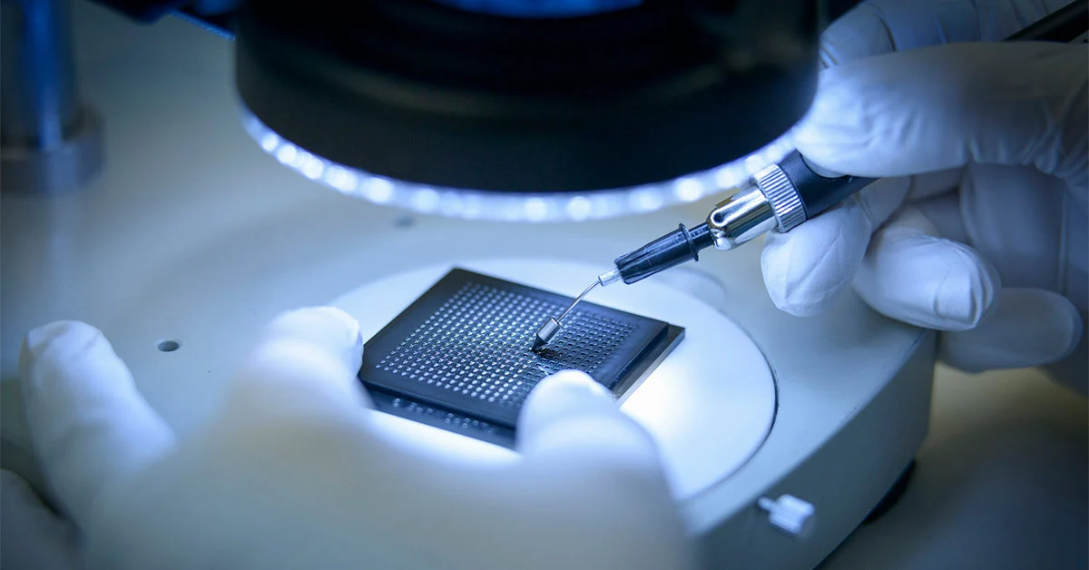
An advanced packaging facility is a specialized factory that uses cutting-edge techniques to assemble complex electronic devices, primarily semiconductors. Advanced packaging facilities play a crucial role in the semiconductor industry, enabling the development of next-generation electronic devices for diverse applications, from high-performance computing and artificial intelligence to mobile devices and wearable electronics.
About Samsung Electronics
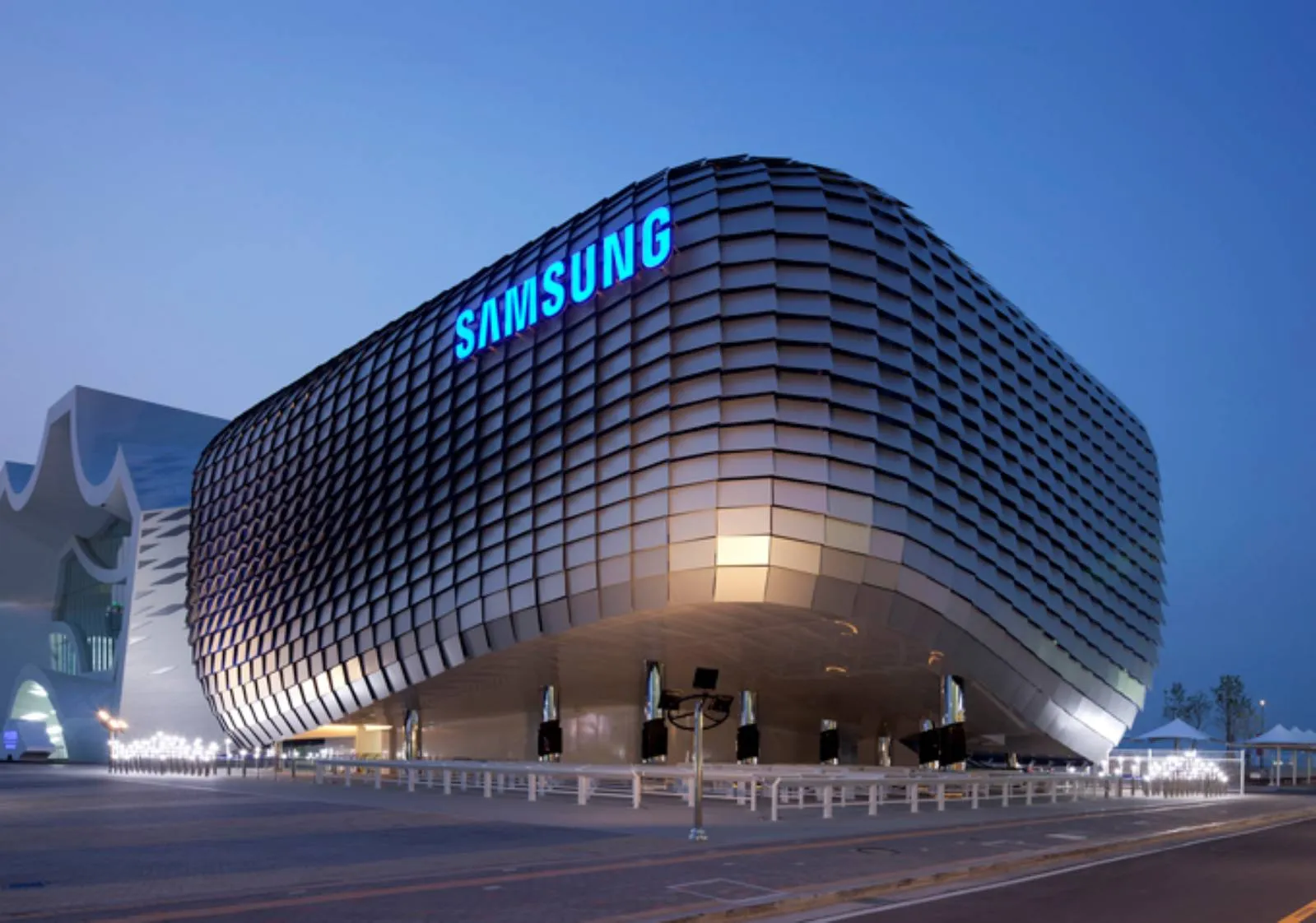
Samsung Electronics is a South Korean multinational electronics company headquartered in Suwon, South Korea. It is the world's largest manufacturer of semiconductors and smartphones, and it consistently ranks among the top global brands. Samsung Electronics has many projects under its pipeline, such as:
Find Upcoming and Ongoing Semiconductor Fabrication Plant Projects in Japan with Ease.
Are you looking for a platform that gives you reliable, high-quality, and timely project insights for Semiconductor Manufacturing Projects in Japan?
Discover the Global Project Tracking (GPT) platform by Blackridge Research, designed to provide you with the most recent Japan Semiconductor Fabrication Plant Projects and Tenders better and faster across various stages of development:
- Upcoming projects
- Tender Notices
- Contract award announcements
- Projects in progress or under construction
- Successfully completed projects.
The user-friendly interface helps you obtain early-stage awareness of projects and find the right business opportunity quickly.
Each project will have all the essential details, such as scope, capacity, CapEx, status, project description, companies involved, funding information, location, periodic updates, important event dates like construction start date, commissioning dates, and key contact information of project owners and stakeholders.
The database is a vital resource for a wide range of entities, including semiconductor manufacturers, EPC Companies, silicon material suppliers, data analytics and software providers, consulting and advisory firms, investors, multilateral banks and financial institutions, and law firms.
Book a Free demo to learn more about the Japan Semiconductor Fab Projects and Tenders database and how we can help you achieve your goals.
Leave a Comment
We love hearing from our readers and value your feedback. If you have any questions or comments about our content, feel free to leave a comment below.
We read every comment and do our best to respond to them all.