


The Biden-Harris Administration has announced a significant funding opportunity for semiconductor manufacturing in the United States. The US government has issued a Notice of Funding Opportunity (NOFO) seeking proposals from eligible applicants for activities to establish and operate a CHIPS Manufacturing USA institute focused on digital twins for the semiconductor market.
This initiative is in line with the Chips and Science Act and aims to bolster US chip technology. The investment is intended to speed up silicon design and engineering and bolster national security. The CHIPS Manufacturing USA Institute is the first manufacturing institute launched by the Department of Commerce under the Biden Administration.
Find Semiconductor Projects and Tenders in USAGet Started Now!
Digital twin-based research can also leverage emerging technology like artificial intelligence to help accelerate the design of new U.S. chip development and manufacturing concepts and significantly reduce costs by improving capacity planning, production optimization, facility upgrades, and real-time process adjustments.
Arati Prabhakar, Assistant to the President for Science and Technology and Director of the White House Office of Science and Technology Policy, emphasized that under President Biden’s leadership, they’re writing a new chapter in semiconductor manufacturing in America.
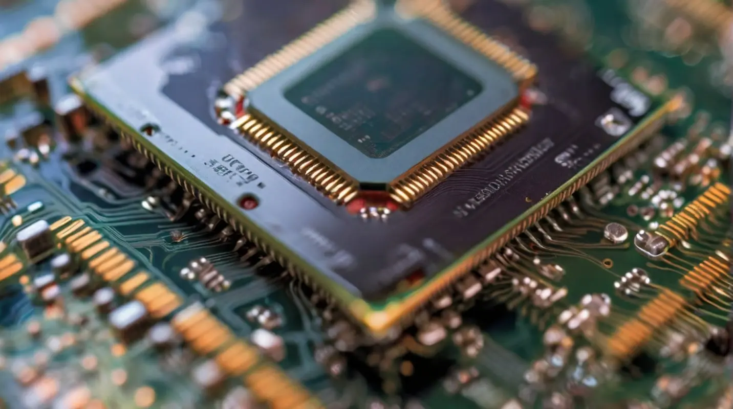
What are Digital Twins in Semiconductor Manufacturing?
Digital twins are virtual models that mimic the structure, context, and behavior of a physical counterpart. The CHIPS for America Program anticipates up to approximately USD 285 million for a first-of-its-kind institute focused on the development, validation, and use of digital twins for semiconductor manufacturing, advanced packaging, assembly, and test processes.
Unlike traditional, physical research models, digital twins can exist in the cloud, which enables collaborative design and process development by engineers and researchers across the country. This creates new opportunities for participation, speeds innovation, and reduces the costs of research and development.
Read: Micron Secures $6.1 Billion Chips Act Funding For Developing Semiconductor Fabs in USA
Connect with decision-makers about Semiconductor Projects in USA for business opportunities.
Subscribe to our Semiconductor Projects in USA Projects and Tender Database to get access to reliable and high-quality insights on upcoming, in-progress, and completed semiconductor projects across the world or in your desired geographical location.
Our user-friendly platform provides essential details, timely updates, key stakeholder contact information, and business opportunities tailored for engineering companies, industry professionals, investors, and government agencies.
Start a free demo to take your business to the next level!
Leave a Comment
We love hearing from our readers and value your feedback. If you have any questions or comments about our content, feel free to leave a comment below.
We read every comment and do our best to respond to them all.