


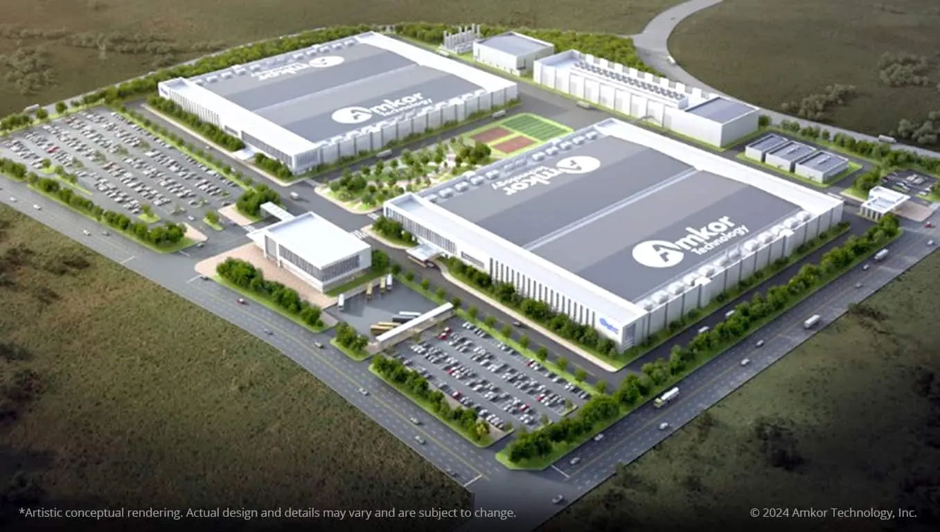
Amkor Technology is developing a USD 2 billion semiconductor packaging and testing facility in Peoria City,Arizona, USA. The Peoria City Council approved a development agreement with Amkor Technology. Through the agreement, Amkor has committed to developing the largest outsourced semiconductor packaging and testing (OSAT) facility in the United States, which will be developed in multiple phases. Furthermore, the project will generate 2,000 new local jobs.
Location and Infrastructure
Amkor will build the campus on 56 acres of land, which will be situated in Five North at Vistancia, Peoria City. The location has a unique mix of skilled workers and adequate infrastructure.
Additionally, public infrastructure associated with the project will be constructed and reimbursed by a three-way agreement with Vistancia Development LLC, Amkor and Peoria, with the city reimbursing up to $3 million toward the cost.
Find Semiconductor Projects and Tenders in USAGet Started Now!
Focus on Packaging and Testing
The Peoria facility will primarily focus on packaging and testing chips produced at the nearby TSMC plant, with Apple as the anticipated largest customer. Semiconductor packaging involves housing the delicate chips in protective enclosures, while testing ensures their functionality before they are integrated into electronic devices.
Government Policy
This multi-billion dollar investment aligns perfectly with the Biden administration's push for domestic semiconductor manufacturing independence. The project has received support from the city of Peoria and the Arizona Commerce Authority, further solidifying its significance. Amkor has also applied for funding through the CHIPS and Science Act, which provides USD 39 billion in incentives for semiconductor manufacturing.
Objectives of the Project
The project aims to establish the largest outsourced semiconductor packaging and testing facility in the United States, contributing to a more robust and self-sufficient domestic chip industry. The project is expected to generate 2,000 new jobs and contribute to the economic growth of Peoria and the surrounding region through construction, operation, and associated activities.
Amkor’s plans for the Peoria facility will provide high-volume, leading-edge technologies for advanced packaging and testing of semiconductors to support critical markets such as high-performance computing, automotive, and communications.
About Amkor Technologies
Amkor Technology, Inc. is a prominent player in the field of semiconductor product packaging and test services. Founded in 1968, Amkor was a pioneer in outsourcing IC packaging and testing. Today, it stands as a strategic manufacturing partner for some of the world’s leading semiconductor companies, foundries, and electronics OEMs,
Amkor provides outsourced semiconductor packaging and test services (OSAT). This includes designing, packaging, and testing integrated circuits (ICs) for various applications. The company has been headquartered in Arizona since 2005, after moving from West Chester, Pennsylvania, in the United States. To further learn about Amkor's upcoming and ongoing semiconductor projects, check out our global semiconductor database.
Find Upcoming and Ongoing Semiconductor Fabrication Plant Projects Around USA with Ease.
Are you looking for a platform that gives you reliable, high-quality, and timely project insights for semiconductor manufacturing projects across USA?
Discover the Global Project Tracking (GPT) platform by Blackridge Research, designed to provide you with the most recent US Semiconductor Fabrication Plant Projects and Tenders better and faster across various stages of development:
- Upcoming projects
- Tender Notices
- Contract award announcements
- Projects in progress or under construction
- Successfully completed projects.
The user-friendly interface helps you obtain early-stage awareness of projects and find the right business opportunity quickly.
Each project will have all the essential details, such as scope, capacity, CapEx, status, project description, companies involved, funding information, location, periodic updates, important event dates like construction start date, commissioning dates, and key contact information of project owners and stakeholders.
The database is a vital resource for a wide range of entities, including semiconductor manufacturers, EPC Companies, silicon material suppliers, data analytics and software providers, consulting and advisory firms, investors, multilateral banks and financial institutions, and law firms
Leave a Comment
We love hearing from our readers and value your feedback. If you have any questions or comments about our content, feel free to leave a comment below.
We read every comment and do our best to respond to them all.