


SK Hynix Assembles Industry's First Commercial High NA EUV Lithography System
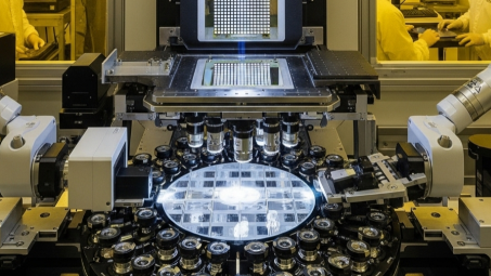
SK hynix Inc. has assembled the industry's first High NA EUV lithography system for mass production at the M16 fabrication plant in Icheon, South Korea. The company announced this milestone development as it prepares to produce next-generation DRAM products using cutting-edge semiconductor manufacturing technology. At a commemorative event for the system assembly, SK hynix's Head of R&D Cha Seon Yong, Head of Manufacturing Technology Lee Byoungki, and ASML's Head of Customer Team SK hynix-Japan Kim Byeong-Chan celebrated the introduction of the equipment designed to produce next-generation DRAM.
The move establishes a foundation for swift development and supply of cutting-edge products to meet customer demand amid intense competition in the global semiconductor industry.
Advanced EUV Technology Implementation
SK hynix has been expanding the scope of EUV adoption for production of the most advanced DRAM since first introducing the technology in 2021 for the 1anm, the fourth generation of the 10nm tech. The assembly of this next-generation technology system that outperforms existing EUV equipment comes as the company prepares for the industry's requirement for extreme scaling and high density.
The TWINSCAN EXE: 5200B represents the first model for volume production of ASML's High NA EUV product line. This system enables printing of transistors 1.7 times smaller and achievement of transistor densities 2.9 times higher compared with the existing EUV system. The new technology delivers a 40% improvement in the NA to 0.55 from 0.33.
40+ reviews
Find the Latest Semiconductor Fabrication Plant Projects in South Korea
Gain exclusive access to our industry-leading database of Semiconductor Fabrication Plant opportunities with detailed project timelines and stakeholder information.
Collect Your Free Leads Here!
No credit cardUp-to-date coverage
Joined by 750+ industry professionals last month
Manufacturing Process Improvements
With the adoption of the new system, SK hynix plans to simplify the existing EUV process and accelerate the development of next-generation memory to advance product performance and cost competitiveness. The sophisticated process technology to scale memory cells is critical to advance productivity and product performance, as a more sophisticated pattern leads to an increase in the number of chips produced from a wafer and an improvement in power efficiency and performance.
The company aims to develop its position in the high-value memory product market and make its technological leadership stronger through this advanced manufacturing capability.
Industry Partnership and Strategic Vision
SK hynix aims to enhance credibility and stability of the global supply chain through close collaboration with business partners. ASML's Kim emphasized the significance of this technology advancement, stating that “High NA EUV is a critical technology that opens the next chapter of the semiconductor industry.” He added that “ASML will closely collaborate with SK hynix to bring forward the innovation of the next-generation memory.”
SK hynix's Cha expressed the company's expectations for the new infrastructure, saying, “We expect the addition of the critical infrastructure to bring our technological vision we have been pursuing into reality.” He further stated that “We aim to enhance our leadership in the AI memory space with the cutting-edge technology required by the fast-growing AI and next-generation computing markets.”
Connect with Decision-makers about the Latest Semiconductor Fabrication Plant Projects in South Korea for business Opportunities.
Subscribe to our database on Semiconductor Fabrication Plant Projects and Tenders in South Korea to get access to reliable and high-quality insights on upcoming, under-construction, and completed Semiconductor Fabrication Plant Projects across the world or in your desired geographical location.
Our user-friendly platform provides essential details, timely updates, key stakeholder contact information, and business opportunities tailored for engineering companies, industry professionals, investors, and government agencies.
Leave a Comment
We love hearing from our readers and value your feedback. If you have any questions or comments about our content, feel free to leave a comment below.
We read every comment and do our best to respond to them all.