


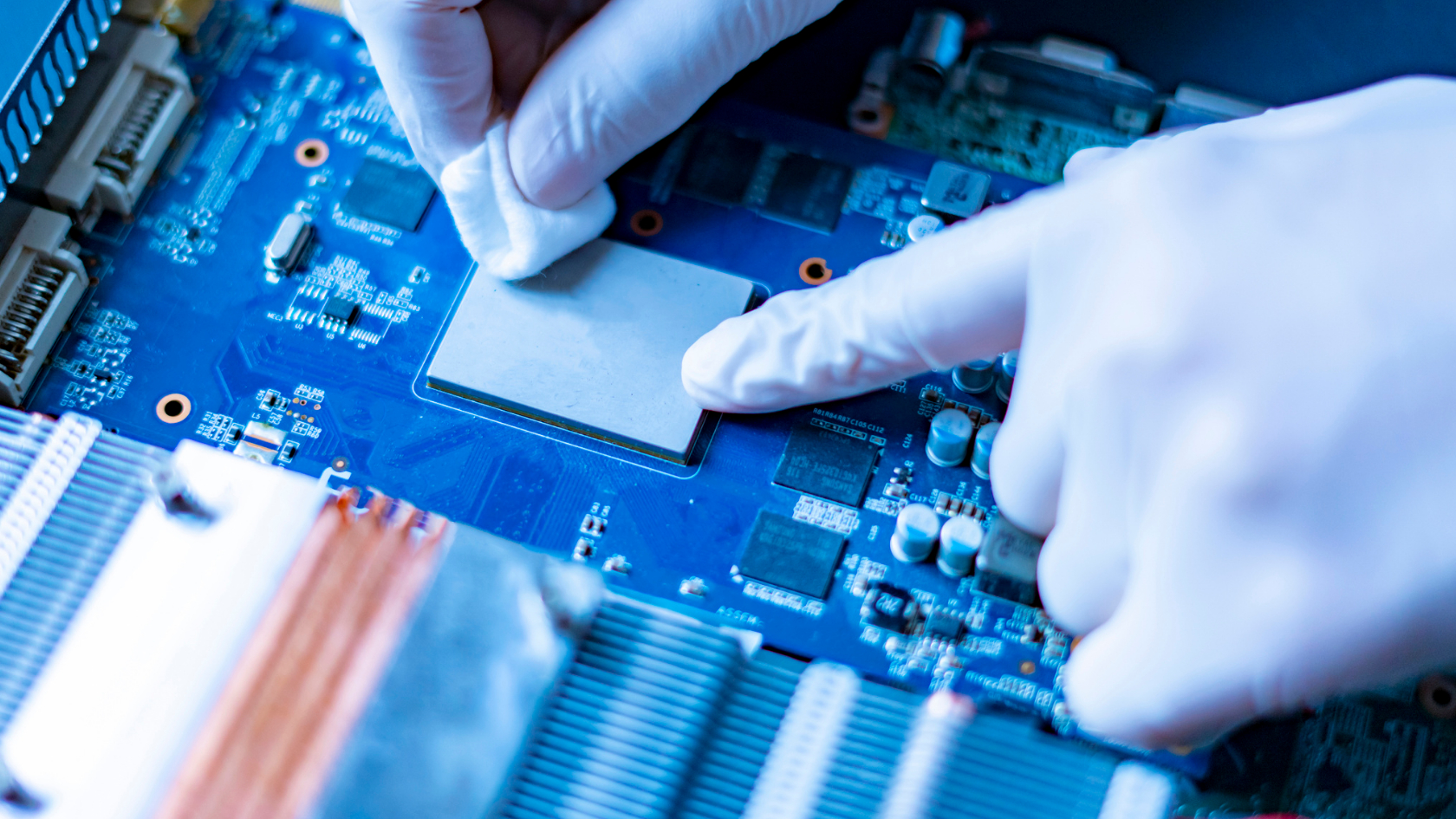
Union Minister Rajeev Chandrasekhar inaugurated the Synopsys Chip Design Center at DLF Park in Noida. It is expected to be the second-largest design center for Synopsys globally, showcasing India's growing talent pool and potential in the semiconductor sector.
Established in 1986, Synopsys widely commercialized logic synthesis, revolutionizing the creation of digital designs from language descriptions. This capability propelled the transition of computer-aided design (CAD) into the electronic design automation (EDA) era, facilitating the scaling of digital complexity in line with Moore’s law.
Find Semiconductor Projects and Tenders in IndiaGet Started Now!
Synopsys has consistently expanded its product portfolio and market position through substantial investments in research and development, coupled with approximately 120 strategic acquisitions. Today, Synopsys is a leading name in EDA, playing a pivotal role in advancing digital chips within the technology ecosystem.
The establishment of the Synopsys Design Center is expected to create high-skilled jobs in areas like chip design, verification, and manufacturing. It will also provide Indian engineers with the opportunity to work on cutting-edge chip design projects.
During the inauguration, Minister Chandrasekhar discussed the expanding ecosystem of fabless chip design and innovation in India. He also expressed appreciation for Synopsys's contribution to the ecosystem and underscored the significance of design in India.
This development is a positive sign for India's aspirations to become a major player in the global semiconductor market. With continued government support and private sector investment, India has the potential to establish itself as a leading destination for chip design and manufacturing.
What are electronic design automation (EDA) tools?
Electronic design automation (EDA) tools are a suite of software programs used to design, validate, and manufacture integrated circuits (ICs), commonly known as chips. These tools are the digital equivalent of blueprints and construction equipment for the microscopic world of chip fabrication. They automate and optimize various tasks that would be too complex or time-consuming for humans to do manually.
About Synopsys
Synopsys is a leading American electronic design automation (EDA) company that provides tools and services for designing and testing semiconductor chips. They are headquartered in Sunnyvale, California, and have a global reach with employees in over 100 countries. They play a crucial role in the development of the cutting-edge technologies shaping our "Smart Everything" world.
Find Upcoming and Ongoing Semiconductor Fabrication Plant Projects in India with Ease.
Are you looking for a platform that gives you reliable, high-quality, and timely project insights for Semiconductor Manufacturing Projects in India?
Discover the Global Project Tracking (GPT) platform by Blackridge Research, designed to provide you with the most recent India Semiconductor Fabrication Plant Projects and Tenders better and faster across various stages of development:
- Upcoming projects
- Tender Notices
- Contract award announcements
- Projects in progress or under construction
- Successfully completed projects.
The user-friendly interface helps you obtain early-stage awareness of projects and find the right business opportunity quickly.
Each project will have all the essential details, such as scope, capacity, CapEx, status, project description, companies involved, funding information, location, periodic updates, important event dates like construction start date, commissioning dates, and key contact information of project owners and stakeholders.
The database is a vital resource for a wide range of entities, including semiconductor manufacturers, EPC Companies, silicon material suppliers, data analytics and software providers, consulting and advisory firms, investors, multilateral banks and financial institutions, and law firms.
Leave a Comment
We love hearing from our readers and value your feedback. If you have any questions or comments about our content, feel free to leave a comment below.
We read every comment and do our best to respond to them all.