


A semiconductor foundry or fab manufactures chips for other companies. Foundries like TSMC (Taiwan Semiconductor Manufacturing Co), GlobalFoundries, and Samsung Foundry manufacture for fabless companies like Nvidia and Qualcomm, which solely design semiconductor chips; they also manufacture for Integrated Device Manufacturers (IDMs) and other companies.
On Converse, IDMs (Integrated Design Manufacturers) like Samsung and Intel design and manufacture semiconductor chips for their products and their clientele.
Semiconductor chips are one of the key components powering automobiles, electronics, data storage, wireless communication, and artificial intelligence.
Evolution of Semiconductor Foundries
Foundries that produce microchips for semiconductor companies were an innovative business model founded by Dr. Morris Chang in 1987, who established the world's first dedicated semiconductor foundry company - TSMC.
Earlier, companies designed and manufactured their own chips. TSMC's taking over the complexity of chip manufacturing boosted several fabless startups and system houses' IC designs that accelerated semiconductor usage and growth, thus integrating them into our lives through various sectors.
Over time, the semiconductor chips evolved from matured nodes of node size greater than 28 nm (nanometers) (28nm, 40 nm, 90 nm, and above) to new cutting-edge advanced nodes that are less than 16-14 nm ( 7nm, 5nm, and 2nm).
The photolithography process is a part of the semiconductor wafer fabrication process that prints tiny circuit patterns onto a wafer to create microchips. It has evolved along with process node technology. A new lithography called EUV (Extreme Ultra Violet) with a 13.5 nm ultraviolet light is being developed to design cutting-edge advanced process node technology of 7nm or less. It varies from the traditional DUV (Deep Ultra Violet) lithography, which uses a 193 nm Arf laser for matured nodes of 28 nm and more.
How Semiconductor Foundries Work: Process & Technology
The semiconductor foundry business specializes in solely manufacturing integrated circuits (ICs) designed by a fabless company. Here's how semiconductor foundries work:
Collaboration with Fabless Companies: A semiconductor foundry business collaborates with a fabless company that designs and doesn't manufacture chips. These companies provide the design for production to the foundry.
Example: TSMC—Fab 18 in Taiwan manufactures chips for fabless companies such as Apple, Qualcomm, NVIDIA, and AMD.
Fabless companies use EDA (Electronic Design Automation) to design chips that define the chip's circuit layout, performance characteristics, and design rules. Once finalized, the design is handed over to the foundry for production, which manufactures the chip using a wafer fabrication process.
Example: TSMC—Fab 18 in Taiwan manufactures chips for fabless companies such as Apple, Qualcomm, NVIDIA, and AMD.
Semiconductor Wafer Fabrication Process
The semiconductor wafer fabrication process is a multi-step procedure that integrates circuits and semiconductor devices. It includes several steps, such as ingot growth, slicing, Edge grinding, Lapping, etching, polishing, and cleaning. This process includes the conversion of raw silicon wafers into semiconductor chips.
Semiconductor Foundry Technology
The semiconductor fabrication process includes a process called transistor type, which includes three types: Planar CMOS, FinFet, and GAAFet. The Planar CMOS was used to design matured nodes with process nodes more than 14nm, whereas Finfet and GAAfet are used for advanced nodes less than 14nm nodes. A clear breakdown is given as follows:
| Feature | Planar CMOS Transistor | FinFET (Fin Field-Effect Transistor) | GAAFET (Gate-All-Around Field-Effect Transistor) |
| Structure | It has a 2D structure for transistor | It uses a 3D fin structure that is more effective than Planar CMOS transistor | It uses nanosheets/nanowires that act as gates covering 4 sides, reducing power leakage |
| Gate Control | The gate is located at the top, leading to high power leakage | There is a partial control that covers the transistor from three sides through 3 gates | Minimum power leakage because it is covered from all sides through four gates. |
| Process Nodes | Matured Nodes (≥28 nm, 40nm, 90nm, above) | Advanced nodes (16nm, 14nm, 10nm, 7nm, 5nm) | Advanced nodes (3nm, 2nm, next-gen transistors) |
| Electrostatic Efficiency | Less efficient due to more power leakage | More efficient than Planar CMOS but cannot be used for smaller nodes | Efficient and suitable for smaller nodes |
| Scaling Feasibility | Suitable for matured nodes | Suitable for nodes upto 5nm | Suitable for smaller nodes less than 5nm. |
| Power and Performance | Maximum power leakage | Less power leakage compared to Planar CMOS | Minimum power leakage |
| Complexity and Cost | Inexpensive and less complex | Less complex and widely used | Complex and expensive but required for smaller and next-gen transistors |
Semiconductor Foundry business V/s OSAT
A Foundry manufactures semiconductor wafers through a fabrication process that includes photolithography, etching, and deposition process for process nodes (advanced & matured) that are sent to OSAT.
OSAT (Outsourcing Semiconductor Assembly & Test) performs the post-fabrication process. This includes assembly, testing, and packaging. OSAT companies assemble the wafers and perform testing processes, which are later packaged using dicing. This process cuts the packed silicon wafers into small dice, which are referred to as "dice." These dice are tested, packed as chipsets, or stacked together as 3D or 2.5D and sent to fabless companies like Apple, Nvidia, and Qualcomm.
What is a Semiconductor Foundry Model?
The semiconductor foundry model is divided into three subcategories, which include fabless companies, pure-play foundries, and IDMs (Integrated Design Manufacturers).
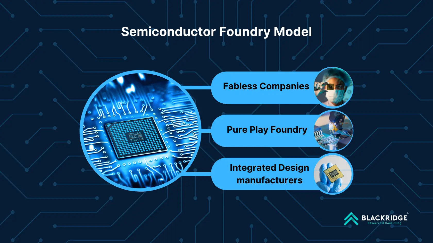
Fabless Companies
Fabless companies solely design ICs and outsource the manufacturing of the chips. This allows the fabless companies to avoid capital-intensive duty and focus more on the innovation of semiconductor chips.
Examples: A few of the top fabless semiconductor companies are NVIDIA and AMD.
Pure-Play Foundry
A pure-play foundry is also referred to as a dedicated foundry manufacturer, and the ICs top its clients. This includes huge capital investment in the fab, expected at USD 10-20 billion per fab plant.
Examples: A few of the major semiconductor TSMC-fab 18 - Taiwan, Samsung Pyeongtaek Campus- South Korea.
IDM (Integrated Design Manufacturers)
IDMs are industry giants that design and manufacture their own chips. These chips are used in their own products and are also supplied to its clients around the world. Samsung and Intel Corporation are the largest IDMs in the world.
Also Read: Global Top 10 Largest Semiconductor Companies [2023]
Key Players in the Semiconductor Foundry Business
Taiwan Semiconductor Manufacturing Company (TSMC) and Samsung Electronics lead the semiconductor market in the foundry business model based on their revenue in 2024. Below is the list of Top Semiconductor Foundry Companies in the world ranked based on revenues in 2024:
| Company | Founded In | Headquarters | Company Type | Annual Revenue Till September 2024 |
| TSMC (Taiwan Semiconductor Manufacturing Company) | 1987 | Taiwan | Pure Play Foundry | USD 64.3 Billion |
| Samsung Electronics | 1969 | South Korea | Integrated Device Manufacturer | USD 58.1 billion |
| UMC (United Microelectronics Corporation) | 1980 | Taiwan | Pure Play Foundry | USD 5.43 billion |
| GlobalFoundries | 2009 | USA | Pure Play Foundry | USD 6.750 billion |
| SMIC (Semiconductor Manufacturing International Corporation) | 2000 | China | Pure Play Foundry | USD 2.17 billion |
Get complete insights into the leading semiconductor foundry companies in the world.
Several government initiatives that have driven the semiconductor industry further include the India Semiconductor Mission (ISM), a mission launched in 2021 under which the Semicon India Programme is proposed with a budget of INR 76000 crores that will support investments in semiconductor & display, including foundries, ATMPS/OSAT facilities and design. This mission also includes the DLI - Design Linked Incentive supporting semiconductor design facilities.
In the U.S., the CHIPS & Science Act was launched in 2022 to support domestic manufacturing, research, and innovation of semiconductors in the US.
Market Trends in Semiconductor Industry (2025)
TSMC‘s Joint Venture to Revive Intel’s Foundry Business in the U.S.
On 12th March 2025, TSMC pitched US chip designers Nvidia, AMD (Advanced Micro Devices), and Broadcom to take stakes in the joint venture (JV) to operate Intel's factories.
Through this joint venture, TSMC aims to operate Intel's foundry division to make them more adapted to customer needs. The stake of TSMC in the JV is expected to be not more than 50%. This deal is still in the early stage and needs to be approved by US President Donald Trump which doesn't want Intel's foundry division to be owned or operated by a foreign entity.
A major driving force for this joint venture is the net loss of USD 18.8 billion, reported with a book value of USD 108 billion as of 31st December 2024.
TSMC’s USD 100 Billion Investment in U.S. Chips
On 4th March 2025, TSMC announced its commitment to invest USD 100 billion to build new semiconductor manufacturing plants in the US.
Also Read: A Complete List of TSMC Fabs
President Trump Ends USD 52.7 Billion CHIPS Act
On 4th March 2025, President Donald Trump announced the ending of the CHIPS and Science Act of USD 52.7 billion. This act supported subsidies for semiconductor chip manufacturing and production in the US. President Trump called an end to this act and suggested the money could be used to reduce debt and encourage tariffs on domestic chip production instead of subsidies.
Emerging Alternatives to Traditional Semiconductor Chips
As the demand for semiconductors rises, new computing technologies emerge as potential alternatives to traditional semiconductor chips. Below listed are a few of the innovative semiconductor technologies.
Photonic Chips
These chips use photons (light) for data processing and transmission, while semiconductor chips use electronic signals for operations. This improves the chip's overall speed and efficiency. The use of light over electronic signals reduces the risk of heating and excess power consumption.
GaN and SiC chips
GaN (Gallium Nitride) and SiC (Silicon Carbide) chips are known to feature high-frequency, high-power, and high-temperature resistance compared to traditional semiconductor chips.
GaN and SiC chips offer high-temperature resistance thus ensuring lower energy loss, making it viable to use in EVs and power applications.
Quantum Computing Chips
These advanced chips use qubits instead of binary bits, making them efficient for parallel computing. Major companies like IBM, Google, Intel, and Microsoft are hugely investing in and developing innovations in quantum computing chips.
On 19th February 2025, Microsoft launched its Majorana 1, which is the world's first quantum processor using topological qubits that will allow the processor to scale up to 1 million qubits in a compact processor size of 10cm x 10 cm. This can be used in cryptography, quantum simulations, AI and many more.
The semiconductor industry relied on Moore's Law - developed by Gordon Moore, co-founder of Intel, which states that no of transistors on a microchip doubles once every two years.
However, with chips reducing to the size of 3-2nm process nodes, heating issues
and manufacturing complexity has led the semiconductor industry to develop alternative solutions like photon and quantum computing.
Conclusion
The semiconductor foundry business plays a pivotal role in manufacturing semiconductor wafers through a fabrication process that empowers fabless companies to innovate and design high-performance, AI-driven, power-efficient chips.
Emerging technologies like photonic chips, quantum computing, GaN, and SiC chips are changing the dynamics of the global semiconductor industry, addressing key challenges such as power efficiency, temperature challenges, and manufacturing complexity due to miniaturization of chips.
While top industry players like TSMC, Samsung, and Intel foundries continue to fulfill global semiconductor chip demand, innovations like photonic chips and quantum computing chips are ensuring next-gen semiconductors that promise faster computing power.
Also Read: List of Largest Semiconductor Fabs in the World (2025)
Get Exclusive Insights on Global Semiconductor Fab Plants!
Looking for real-time updates on global semiconductor fab projects? Explore Blackridge Research’s Global Semiconductor Fabrication Plants database and access:
- Upcoming Projects
- Tender Notices
- Contract Awards
- Ongoing Developments
- Completed Projects
Whether you're an EPC company, investor, consultant, or financial institution, our database provides the market intelligence you need to stay ahead.
Book a Free Demo today and discover how this database can help you make informed, data-driven decisions!


Leave a Comment
We love hearing from our readers and value your feedback. If you have any questions or comments about our content, feel free to leave a comment below.
We read every comment and do our best to respond to them all.