
Table of Contents
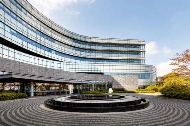
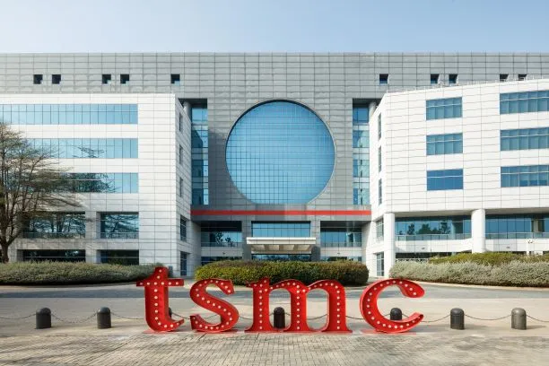
Taiwan Semiconductor Manufacturing Company (TSMC) is the world’s largest and most advanced pure-play foundry. It operates more than 20 fab plants, including its advanced backend fab plants across the globe. With major fab plants located in Taiwan, it has laid successful milestones in the USA and China.
From mature nodes to advanced nodes smaller than 2 nm, TSMC plays a critical role in powering industries like AI, automotive, smartphones, and IoT (Internet of Things).
In this blog, we have covered a complete list of TSMC fabs with their locations, advanced backend fabs, upcoming projects and investments, including advanced plants like TSMC Fab 18, Fab 14, and Fab 21.
List of TSMC Fabs
Wafer Size | Fab Name | Location | Capacity (wafers per month) | Process Nodes | Lithography |
|---|---|---|---|---|---|
12-inch (300mm) | Fab 12 A | Hsinchu, Taiwan | 25,000 | 0.15 µm, 0.13 µm, 0.10 µm | DUV |
Fab 12 B | Hsinchu, Taiwan | NA | 28 nm, 22 nm | DUV | |
Fab 14 | Southern Taiwan Science Park, Tainan | 1,37,000 | 20 nm | DUV | |
Fab 15 | Taiwan Science Park, Taichung | 100,000 | 20 nm | DUV | |
Fab 16 | Pukou Economic Development Zone | 20,000 | 16 nm | DUV | |
Fab 18 | Tainan, Taiwan | More than 1 million | 5nm, 3nm | EUV | |
Fab 21 | Arizona, USA | NA | 5 nm, 4 nm, 3nm, A16 and 2 nm | EUV | |
JASM Kumamoto Plant | Kikuyo, Kumamoto Prefecture, Japan | 100,000 | 40 nm, 22 nm, 28 nm, 12 nm, 16 nm, and 6 nm, 7 nm | DUV, EUV | |
8-inch (200mm) | Fab 3 | Hsinchu, Taiwan | 25,000-30,000 | 80 nm, 250 nm, 350 nm, 0.5μm to 0.18μm | DUV |
Fab 5 | Hsinchu, Taiwan | 40,000 | 80 nm, 250 nm, 350 nm, 0.5 μm to 0.18 μm, 0.25 and 0.22 microns | DUV | |
Fab 6 | Southern Taiwan Science Park, Tainan | 50,000 | 80 nm, 250 nm, 350 nm, 0.5μm to 0.18μm, 0.35 and 0.30 μm | DUV | |
Fab 8 | Hsinchu, Taiwan | NA | 0.35 and 0.30 microns | DUV | |
Fab 10 | Shanghai, China | 50,000 | 130 nm, 180 nm, and 250 nm, 0.25 and 0.35-micron | DUV | |
TSMC Washington (Fab 11) | Washington | NA | 0.35 to 0.16 microns | DUV | |
6-inch (150mm) | Fab 2 | Hsinchu, Taiwan | NA | Matured Nodes (not specified) | DUV |
| Fab Name | Location | Technology |
|---|---|---|---|
Advanced Backend Fabs | Advanced Backend Fab 1 | Taiwan | Wire-bonding, Standard Wafer-Level Packaging |
Advanced Backend Fab 2 | Taiwan | Flip-chip bonding, Wire-bonding | |
Advanced Backend Fab 3 | Taoyuan City, Taiwan | Backend Operations | |
Advanced Backend Fab 5 | Central Taiwan Science Park, Taiwan | Flip-chip, Chip-on-Board | |
Advanced Backend Fab 6 | Zhunan Township, Miaoli, Taiwan | 3DFabric™, SoIC, InFO, CoWoS, Advanced Testing |
TSMC Fabs Breakdown
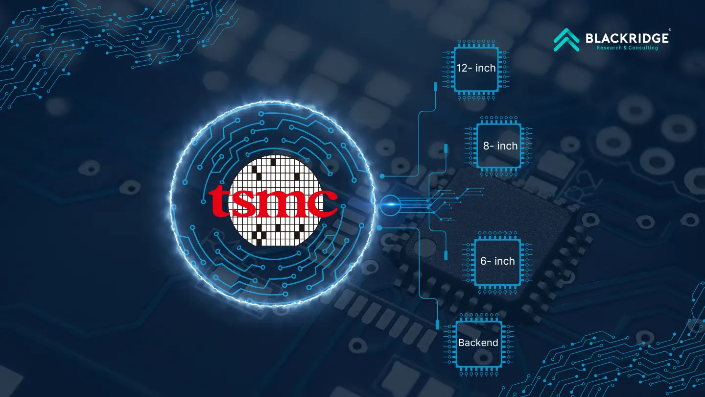
TSMC has fabs in the USA, China, and Taiwan. These fabs are divided based on different semiconductor wafer sizes, such as 12-inch, 8-inch, and 6-inch. TSMC also features backend fabs that use several technologies based on the node size. Keep reading to know more.
12-inch FABs
TSMC Fab 12A
Category | Details |
|---|---|
Fab Name | TSMC Fab 12A |
Location | Hsinchu Science Park, Taiwan |
Year Established | 2002 |
Wafer Size | 12 inch |
Process Nodes | 0.15 µm, 0.13 µm, 0.10 µm |
Production Capacity | 25,000 wafers per month |
Investment Cost | USD 2 billion (estimated) |
Lithography | DUV lithography |
TSMC Fab 12A is a 12-inch fab plant located in Hsinchu Science Park. It manufactures 300 mm wafers that began production in early 2002. This 12-inch fab plant produces 0.15 and 0.13 micron process technologies and 0.10 micro feature sizes. It specializes in logic, memory, and chipset products. The plant's capacity is about 25,000 12-inch wafers per month.
TSMC broke ground for this 300 mm fab plant in December 1999 and finished the construction of this plant by the end of 2000. The equipment was moved into the plant in 2001. It began its production in early 2002.
This plant also features a small capacity for R&D (research & development). The plant is built with an investment cost of more than USD 2 billion (estimated).
TSMC Fab 12B
Category | Details |
|---|---|
Fab Name | TSMC Fab 12B |
Location | Hsinchu Science Park, Taiwan |
Year Established | 2009-10 |
Wafer Size | 12 inch |
Process Nodes | 28 nm, 22 nm |
Production Capacity | Not announced |
Investment Cost | Not announced |
Lithography | DUV lithography |
The TSMC fab 12B is a 12-inch wafer plant of TSMC located in Hsinchu Science Park, Taiwan. It is a part of the 300mm Fab 12 plant developed by TSMC in Taiwan.
Fab 12 plant has multiple phases, phase 1 and phase 2 facilities manufacture 28 nm process technology, whereas phase 4 & 5 are TSMC's latest production facilities. The phase 4 & 5 manufacture 22 nm and more advanced process technologies. Phase 4, which broke ground at the end of the Chinese New Year (January 2009), began volume production in 2009. Phase 5 began construction at the end of 2009 and entered volume production in Q3 of 2019.
Apart from production, Fab 12 also operates as an R&D for advanced process technologies. Phases 4 & 5 have a total site area of 7.83 hectares and a clean room area of 22,700 square meters, equivalent to 3 soccer fields.
On 9th August 2012, TSMC Fab 12, phases 4 & 5 received ISDO 50001 Energy Management System established by the International Standards Organization (ISO), which certifies that Fab 12 will conserve 50 million kilowatt hours of electricity and eliminate 30,000 tons of carbon emissions per year in 2012 as per the ISO 50001 standards.
TSMC Fab 14
Category | Details |
|---|---|
Fab Name | TSMC Fab 14 |
Location | Southern Taiwan Science Park, Tainan |
Year Established | 2004 |
Wafer Size | 12 inch |
Process Nodes | 20 nm |
Production Capacity | 1,37,000 wafers per month |
Investment Cost | Not announced |
Lithography | DUV lithography |
TSMC Fab 14 is a second 12-inch fab plant of TSMC located in Southern Taiwan Science Park, Tainan. It specializes in manufacturing 20 nm and more advanced technologies. It is planned and built in several phases. Phase 5, TSMC's second 20 nm plant, broke ground on 9th April 2012 and began production in early 2014.
Phase 1 of fab 14 began volume production in 2004, and the total capacity of the first four phases (1- 4) is 550,000 12-inch wafers per quarter.
The total cleanroom area of fab 14 phases 5 and 6 combined is 87,000 square meters, equivalent to more than 11 soccer fields. On 9th August 2012, TSMC Fab 14 received ISO 50001 Energy Management System certification, certifying that this plant will conserve 50 million kilowatt-hours of electricity and eliminate 30,000 tons of carbon emissions per year as of 2012.
TSMC Fab 15
Category | Details |
|---|---|
Fab Name | TSMC Fab 15 |
Location | Taiwan Science Park, Taichung |
Year Established | 2011 |
Wafer Size | 12-inch wafer |
Process Nodes | 20 nm |
Production Capacity | 100,000 wafers per month |
Investment Cost | USD 9 billion (estimated) |
Lithography | DUV lithography |
TSMC Fab 15 is Taiwan Science Park, Taichung. It consists of Fab 15A and Fab 15B. Fab 15 A is a semiconductor fab plant, whereas Fab 15B is built to maintain and promote biological diversity.
Fab 15 A is built with a capacity of 100,000 12-inch wafers per month. It is equipped with 28 nm technology. It is spread across a site of 18.4 hectares with an estimated investment of NT$ 300 billion (USD 9 billion). It has a building area of 430,000 square meters and a cleanroom area equal to the size of 14 football pitches.
It was built in multiple phases, with phase 1 completion in June 2011. It began volume production of 28 nm and 40 nm products in Q1 of 2012. In April 2015, it broke ground for the expansion of Fab 15. On the other hand, Fab 15 B and the Department of Forestry of National Chung Hsing University in Taichung restored about 204 plants in the close-to-nature forest by March 2020.
TSMC's Fab 15 is built as a green building, promoting greenbelt and fostering ecosystem-specific site characteristics. This concept of green building for TSMC fab 15 was designed and planned by JJP Architects and Planners. It was designed during the period of February 2015 - July 2017. It was awarded the "Outstanding Green Building Design Award" in 2021.
TSMC Fab 16
Category | Details |
|---|---|
Fab Name | TSMC Fab 16 |
Location | Pukou Economic Development Zone. |
Year Established | 2018 |
Wafer Size | 12-inch wafer |
Process Nodes | 16 nm |
Production Capacity | 20,000 wafers per month |
Investment Cost | Not announced |
Lithography | DUV lithography |
TSMC Fab 16 is owned by a TSMC subsidiary, TSMC Nanjing Company Limited. It is located at the Pukou Economic Development Zone. This 12-inch fab plant has a capacity of 20,000 12-inch wafers per month.
It specializes in 16 nm process technology and entered volume production in the second half of 2018. On 28th March 2016, TSMC and the Nanjing, China municipal government signed an investment agreement valued at USD 3 billion for this plant. L&K Engineering (Suzhou) Co. Ltd is a key company in building cleanroom spaces in TSMC Nanjing.
TSMC Fab 18
Category | Details |
|---|---|
Fab Name | TSMC Fab 18 |
Location | Tainan, Taiwan |
Owner | Taiwan Semiconductor Manufacturing Company |
Year Established | 2022 |
Wafer Size | 12-inch (300mm) |
Process Nodes | 5 nm, 3 nm |
Production Capacity | More than 1 million wafers per month |
Investment Cost | USD 60.98 billion |
Lithography | EUV Lithography |
TSMC Fab 18 is a 12-inch wafer plant located in Southern Taiwan Science Park in Tainan. This GIGAFAB® facility specializes in 5 nm and 3 nm process technology. It entered volume production on 29th December 2022.
This plant is built in 8 phases with a cleanroom area of 58,000 square meters, which is double the size of a standard logic fab. Phase 1 began construction in 2019 and entered volume production by 2020, phase 2 began construction in Q3 and entered production in 2020; likewise, phase 3 began construction in 2019 and entered volume production in 2021.
This plant has an annual capacity exceeding one million 12-inch wafers. Fab 18 is constructed at an estimated cost of NT$1.86 trillion (USD 60.98 Billion).
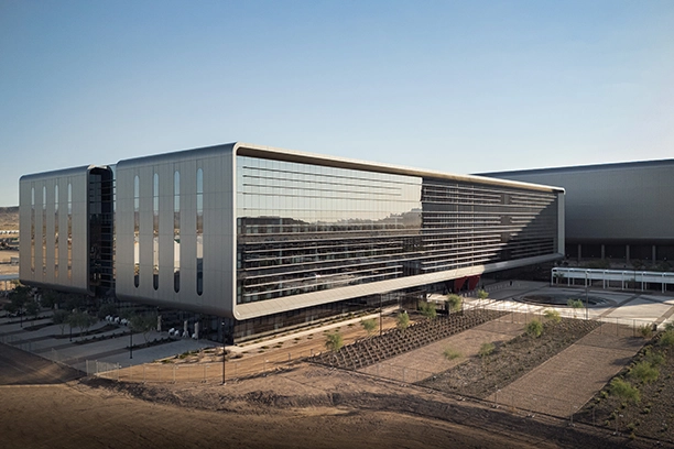
TSMC Fab 21
Category | Details |
|---|---|
Fab Name | TSMC Fab 21 |
Location | Phoenix, Arizona |
Year Established | 2024 - 2030 |
Wafer Size | 12-inch wafer |
No of Fab plants | 3 (2 under construction) |
Process Nodes | 5 nm, 4 nm, 3nm, A16 and 2 nm |
Production Capacity | Not Announced |
Investment Cost | USD 40 Billion |
Lithography | EUV lithography |
TSMC Fab 21, Arizona, is one of TSMC's major semiconductor fab plants in the U.S. Located in Phoenix, Arizona, it will have three fab plants that collectively manufacture tens of millions of leading-edge logic chips used in 5G/6G smartphones, autonomous vehicles, and high-performance computing and AI applications. Additionally, these chips are used in CPUs and GPUs used for machine learning.
The three manufacturing fabs under TSMC Arizona include:
Fab 1: 4nm and 5nm FinFET process technologies
Fab 2: 3nm FinFET process technologies
Fab 3: A16 and 2nm nanosheet process technologies
The TSMC Arizona's Fab 1 construction began in April 2021 and entered volume production of N4 (4 nm process technology) in Q4 of 2024. The fab 2 with N3 (3 nm process technology) is expected to enter volume production in 2028. The third fab is expected to produce 2 nm or even more advanced process technology by the end of the decade.
TSMC Arizona was first announced by TSMC with an investment of USD 12 billion in May 2020. In December 2022, the company announced its plans to increase the total investment to USD 40 billion. In April 2024, the U.S. Department of Commerce issued a direct funding of USD 6.6 billion under the CHIPS and Science Act. It also received a loan amount of USD 5 billion from the CHIPS Program Office (CPO) under "CHIPS Notice of Funding Opportunity for Commercial Fabrication Facilities."
In January 2025, TSMC announced that TSMC Arizona started high-volume N4 Process node production with a yield rate comparable to its advanced fabs in Taiwan.
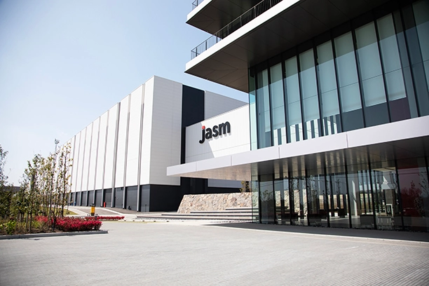
JASM Kumamoto Plant
Category | Details |
|---|---|
Fab Name | JASM Kumamoto Plant |
Location | Kikuyo, Kumamoto Prefecture, Japan |
Year Established | 2024 - 2030 |
Wafer Size | 12-inch wafer |
No of Fab plants | 3 ( 2 under construction) |
Process Nodes | 40 nm, 22 nm, 28 nm, 12 nm, 16 nm, and 6 nm, 7 nm |
Production Capacity | 100,000 wafers per month |
Investment Cost | USD 40 Billion |
Lithography | EUV lithography |
JASM is a joint venture between Sony Semiconductor Solutions, Denso, and Toyota. This joint venture owns and built the first semiconductor fab plant in Japan. TSMC holds a major stake in this plant. This plant features 22 nm, 28 nm, 12 nm, and 16 nm process technologies for Logic Integrated Circuits (ICs). It is located in Kikuyo, Kumamoto Prefecture, Japan.
The first fab began its operation in 2024 and was built with an investment of USD 20 billion, funded by the Japanese government. The JASM’s Kumamoto facility, with two fab plants, is expected to deliver a production capacity of more than 100,000 12-inch wafers per month.
On 6th February 2024, TSMC announced its plans to build a second fab plant at Kumamoto Prefecture with an investment of USD 13.5 billion.
This includes process technology nodes from 40 nm, 22 nm, 28 nm, 12 nm, 16 nm, and 6 nm, 7 nanometre process technologies. These will be used in automotive, industrial, consumer, and HPC (High Performing Computing) applications.
TSMC announced its plans to construct a third fab plant in Kumamoto, Japan, with an investment of USD 20 billion. This plant will feature cutting-edge 3-nanometer technology used in the latest smartphones.
8-inch fabs
TSMC Fab 3
Category | Details |
|---|---|
Fab Name | TSMC Fab 3 |
Location | Hsinchu Science Park, Hsinchu |
Year Established | 1990s |
Wafer Size | 8 - inch wafer |
Process Nodes | 80 nm, 250 nm, 350 nm, 0.5μm to 0.18μm. |
Production Capacity | 25,000 to 30,000 wafers per month |
Investment Cost | Not Announced |
Lithography | DUV lithography |
TSMC fab 3 is a 200 mm (8 inch) fab plant located at Hsinchu Science Park, Hsinchu, Taiwan. It is TSMC's first 8-inch fab facility specializing in mature process technologies (80 nm, 250 nm, and 350 nm) It was built in the 1990s and specializes in process nodes transitioning from 0.5μm to 0.18μm.
The plant is estimated to have a production capacity of around 25,000 to 30,000 8-inch wafers per month, with a total area of about 137,000 square meters.
TSMC Fab 5
Category | Details |
|---|---|
Fab Name | TSMC Fab 5 |
Location | Hsinchu Science Park in Hsinchu |
Year Established | 1997 |
Wafer Size | 8 - inch wafer |
Process Nodes | 80 nm, 250 nm, 350 nm, 0.5 μm to 0.18 μm, 0.25 and 0.22 microns |
Production Capacity | 40,000 wafers per month |
Investment Cost | Not Announced |
Lithography | DUV lithography |
TSMC Fab 5 is an 8-inch wafer plant located at Hsinchu Science Park in Hsinchu, Taiwan. This plant specializes in mature process technologies similar to TSMC's fab three plants.
It was established in October 1997, with an estimated capacity of 40,000 8-inch wafers per month by the end of 2000. TSMC's Fab 5 was cited as one of the top 3 Fab in the 2000s by Semiconductor International.
TSMC fab 5 is the company's third 8-inch fab, with construction started in November 1995. During its time, it was the first fab in Taiwan to adopt a design configuration built on two floors of equal size. Its volume production began in early 1998 with a 0.35-micron process node technology. It offered 0.35 and 0.30-micron logic products in 1998 and advanced to 0.25 and 0.22-micron technologies as a technology generation advancement.
TSMC Fab 5 also boasts conservation strategies saving about USD 5 million on operating costs and reducing CO2 emissions by 44,000 tons per year. It received several other recognitions, such as "Outstanding Manufacturer for Energy Conservation" in November 1999 by the Energy Committee of the Ministry of Economic Affairs and “AAA damage prevention and fire safety certificate” by Cigna Insurance in March 1999.
TSMC Fab 6
Category | Details |
|---|---|
Fab Name | TSMC Fab 6 |
Location | Southern Taiwan Science Park, Tainan |
Year Established | 1997 |
Wafer Size | 8 - inch wafer |
Process Nodes | 80 nm, 250 nm, 350 nm, 0.5μm to 0.18μm, 0.35 and 0.30 μm |
Production Capacity | 50,000 wafers per month |
Investment Cost | USD 2.4 billion |
Lithography | DUV lithography |
TSMC Fab 6 is a massive six-story building across 190,000 square feet. It has a production capacity of 50,000 8-inch wafers that entered volume production in 2001. It specializes in mature process technology.
In July 2000, TSMC announced its plans to install the first 12-inch pilot production facility inside its Fab 6 cleanroom facility. On completion, this pilot project began processing silicon wafers in December 2000, producing about 4,500 12-inch wafers a month by November 2001.
Also known as "Big Mac" by TSMC, it was developed with an investment of USD 2.4 billion, which includes USD 2 billion for an 8-inch fab plant and USD 400 million for the 12-inch (300mm) pilot project inside the facility.
TSMC Fab 8
Category | Details |
|---|---|
Fab Name | TSMC Fab 8 |
Location | Hsinchu Science Park, Hsinchu, Taiwan, |
Year Established | 1990s |
Wafer Size | 8 - inch wafer |
Process Nodes | 0.35 and 0.30 microns |
Production Capacity | Not Announced |
Investment Cost | Not Announced |
Lithography | DUV lithography |
TSMC Fab 8 located at the Hsinchu Science Park, Hsinchu, Taiwan, is a 8-inch wafer plant. It specializes in mature nodes (0.35 and 0.30 microns) and was established in the early 1990's.
TSMC China Company Limited, Fab 10
Category | Details |
|---|---|
Fab Name | TSMC Fab 10 |
Location | Shanghai, China |
Year Established | 2004 |
Wafer Size | 8 - inch wafer |
Process Nodes | 130 nm, 180 nm, and 250 nm, 0.25 and 0.35-micron |
Production Capacity | 50,000 wafers per month |
Investment Cost | Not Announced |
Lithography | DUV lithography |
TSMC Fab 10 is a key semiconductor fab plant in Shanghai, China. On 8th June 2003, TSMC China Company Limited signed an agreement with Shanghai’s Songjiang District authorities to build an 8-inch (200 mm) fab plant in Shanghai, China.
TSMC Fab 10 specializes in 0.25 and 0.35-micron processes. It began its trial production of 5,000 wafers on 1st August 2004. In July 2010, TSMC announced its plans to expand the Shanghai 8-inch fab capacity by two-thirds. The expansion led to an increase in production of up to 50,000 wafers per month. Fab 10 focuses on mature nodes such as 130 nm, 180 nm, and 250 nm.
TSMC Washington, LLC, Fab 11
Category | Details |
|---|---|
Fab Name | TSMC Washington (Fab 11) |
Location | Washington |
Year Established | 2000 |
Wafer Size | 8 - inch wafer |
Process Nodes | 0.35 to 0.16 microns |
Production Capacity | Not announced |
Investment Cost | USD 2 billion |
Lithography | DUV lithography |
TSMC Washington, LLC, Fab 11 is one of the biggest TSMC manufacturing sites located around the world. It is a wholly-owned subsidiary of TSMC and focuses on embedded Flash process technology, supporting line - widths ranging from 0.35 to 0.16 microns.
It delivers semiconductor chips to automotive, communications, computing, consumer, industrial, medical, and military/aerospace applications. Earlier, this plant was called WaferTech fab, established in Washington in 1996 with an investment of more than USD 2 billion. In 2000, TSMC, along with investors, took full control of the plant and renamed it TSMC Fab 11.
6-inch fab
TSMC Fab 2
Category | Details |
|---|---|
Fab Name | TSMC Fab 2 |
Location | Hsinchu Science Park, Taiwan |
Year Established | 2000s |
Wafer Size | 6 - inch wafer |
Process Nodes | Mature nodes (not specified) |
Production Capacity | Not announced |
Investment Cost | Not announced |
Lithography | DUV lithography |
The TSMC Fab 2 is a six-inch wafer fab plant located at Hsinchu Science Park, Taiwan. It is the only 6-inch wafer plant owned and operated by TSMC. It features mature nodes, and in April 2004, it reached its maximum utilization, leading to TSMC outsourcing a part of its wafer processing to Mosel Vitelic. This Taiwanese semiconductor company manufactures power discrete power management of IC and analog IC technologies.
TSMC’s Advanced Backend Fabs
TSMC is a leading pure-play foundry of semiconductor wafers offering products of 12-inch, 8-inch, and 6-inch wafer plants. Apart from fab plants, TSMC also specializes in advanced backend fab plants. Currently, TSMC operates 5 advanced backend fab plants. These plants offer varied services such as and are not limited to wafer testing, die cutting, die bonding, wire bonding, final testing, and packaging. The list of the advanced fab plants is as follows:
Advanced Backend Fab 1
Advanced Backend Fab 2
Advanced Backend Fab 3
Advanced Backend Fab 5
Advanced Backend Fab 6
Here is a quick view of the Advanced backend plants:
Advanced Backend Fab Plant | Location | Technology | Details |
|---|---|---|---|
Advanced Backend Fab 1 | Taiwan | Wire-bonding, Standard Wafer-Level Packaging | First advanced backend fab; provides conventional packaging and testing services. |
Advanced Backend Fab 2 | Taiwan | Flip-chip bonding, Wire-bonding | Includes conventional packaging and testing and supports both flip-chip and wire-bonding processes. |
Advanced Backend Fab 3 | Taoyuan City, Taiwan | Backend Operations | Handles major backend operations of semiconductor fab plants. |
Advanced Backend Fab 5 | Central Taiwan Science Park, Taiwan | Flip-chip, Chip-on-Board | Focuses on packaging and testing of electronic chips; specializes in flip-chip and chip-on-board technologies. |
Advanced Backend Fab 6 | Zhunan Township, Miaoli, Taiwan | 3DFabric™, SoIC, InFO, CoWoS, Advanced Testing | Most advanced fab; supports advanced packaging, silicon stacking, and 3DFabric™ integration for improved yield & efficiency. |
Upcoming TSMC Fab Plants
TSMC Arizona
It is currently under expansion with two new plants. the second fab will lead N3 process technology set to be operational by 2030.
TSMC Fab 21
The third fab planned at this TSMC Arizona will manufacture 2nm or even more advanced chips expected to be operational by 2030.
TSMC Plants Kumamoto
TSMC Is building two more fab plants in Kumamoto. The second fab plant is built with an investment of USD 13.5 billion and will manufacture 40 nm, 22 nm, 28 nm, 12 nm, 16 nm, and 6 nm, 7 nanometre process technologies.
It also announced a third fab plant with an investment of USD 20 billion that will manufacture 3 nm process technology used in smartphones.
On 4th March 2025, TSMC announced its plans to expand semiconductor manufacturing in the United States through USD 100 billion. This includes a USD 65 billion investment for the expansion of TSMC Arizona.
On 12th March 2025, TSMC pitched US chip designers Nvidia, AMD, and Broadcom to take stakes in a joint venture to operate US Intel foundries that reported a net loss of USD 18.8 billion as of 31st December 2024.
TSMC Latest News 2025
On 11th august 2025, TSMC announced its consolidated revenue of NT$323.166 billion (US$10.82 billion) in July. This is a 22.5% increase from June and a 25.8% increase compared to July 2024.
On 5th July 2025, TSMC announced it has decided to phase out its GaN (Gallium nitride) semiconductor business in 2 years due to the increased competition from China and decline in profits. In line with this announcement, US-based Navitas Semiconductor will shift its GaN orders from TSMC to PSMC over the next 12 to 24 months.
Reportedly, TSMC announced Q2 2025 revenue of NT$933.8 billion (USD 28.9 billion) which is a 38-39% year-on-year increase. Back on 4th March 2025, TSMC announced its plans to increase U.S. investment in advanced semiconductor manufacturing by USD 100 billion with three new fabs and two advanced packaging facilities and an R&D center.
Conclusion
TSMC continues to stand firm in the pure-play foundry industry. With innovation in fab plants expanding up to 2 nm and less process technology to innovating 3DFabric™ for its most advanced backend fab 6, TSMC stands as the global leader in semiconductor manufacturing. Through advanced and mature nodes, TSMC fabs continue to meet the growing global demand for high-performance, energy-efficient chips.
With advanced facilities like TSMC Fab 18, and Fab 14, and upcoming fabs such as Kumamoto plants and the expansion of TSMC Arizona, TSMC continues to expand its portfolio across countries.
Get Exclusive Insights on Global Semiconductor Fab Plants!
Looking for real-time updates on global semiconductor fab projects? Explore Blackridge Research’s Global Semiconductor Fabrication Plants database and access:
Upcoming Projects
Tender Notices
Contract Awards
Ongoing Developments
Completed Projects
Whether you're an EPC company, investor, consultant, or financial institution, our database provides the market intelligence you need to stay ahead.
Book a Free Demo today and discover how this database can help you make informed, data-driven decisions!


Leave a Comment
We love hearing from our readers and value your feedback. If you have any questions or comments about our content, feel free to leave a comment below.
We read every comment and do our best to respond to them all.