List of Top Semiconductor Fabs In the United States (2025)
Table of Contents
Semiconductor fabs in the US played a pivotal role in positioning the US semiconductor industry as one of the world's most advanced semiconductor manufacturing hubs.
According to the Semiconductor Industry Association, by the end of 2024, the world semiconductor sales hit USD 630.5 billion, which is forecasted to increase to USD 697.2 billion in 2025 and USD 738.6 billion in 2026.
While several other countries like China, Korea, and Japan are competing to capture the market, the US stands strong with the largest market share of 50.4% as of May 2025. The US semiconductor sales reported USD 318.2 billion in 2024 with a compound annual growth rate of 6.7% according to Semiconductor Industry Association.
As the US continues to expand its semiconductor industry through manufacturing and exports, the operational semiconductor fabs play a significant role as the backbone driving this growth. In this blog, we have compiled the list of the largest semiconductor fabs in the US. Keep reading for more!
Top Semiconductor Fabs in the US 2025
Fab Name | Capacity (WSPM) | Developer (Owner / Operator) | Location | Project Status |
East Fishkill (EFK) Fab | 20,000 | ON Semiconductor | East Fishkill, New York, USA | Operational |
GlobalFoundries Fab 8 | 30,000 (expected 60,000 wspm once fully operational) | GlobalFoundries | Malta, New York, USA | Operational; expansion ongoing |
Intel D1X | Not Announced | Intel | Hillsboro, Oregon, USA | Operational; expansion ongoing |
Intel Fab 9, Rio Rancho | Not Announced | Intel | Rio Rancho, New Mexico, USA | Reopened Jan 2024; Operational |
Intel Ocotillo Campus (Fab 42) | Not Announced | Intel | Chandler, Arizona, USA | Operational; Fab 52 & 62 under construction |
Micron Boise Campus | Not Announced | Micron Technology | Boise, Idaho, USA | Under construction; expected operational 2027 |
Samsung Austin Semiconductor (S1 & S2) | 40,000 | Samsung | Austin, Texas, USA | Operational |
Taylor Semiconductor Plant | Not Announced | Samsung | Texas, USA | Under construction; expected operational 2026 |
Texas Instruments RFAB 1 & 2 | Not Announced | Texas Instruments | Richardson, Texas, USA | Operational; expansion ongoing |
TSMC Arizona Fab 21 | 10,000 (full 20,000 wspm by 2026) | TSMC | Phoenix, Arizona, USA | Partially operational; other fabs under construction |
The largest semiconductor fabs in the US are listed in alphabetical order.
40+ reviews
Find the Latest Semiconductor Projects Across United States
Gain exclusive access to our industry-leading database of semiconductor project opportunities with detailed project timelines and stakeholder information.
Collect Your Free Leads Here!
No credit cardUp-to-date coverage
Joined by 750+ industry professionals last month
East Fishkill (EFK) Fab
Category | Details |
Fab Name | East Fishkill (EFK) Fab / Fab 10 |
Location | East Fishkill, New York, USA |
Owner | ON Semiconductor |
Year Established | Originally by IBM as Fab 11; acquired by ON Semiconductor in 2023 |
Wafer Size | 300 mm |
Process Nodes | 40 nm, 65 nm CMOS |
Type of Fab | Image sensor production |
Investment Cost | USD 430 million |
Lithography | DUV Lithography |
The East Fishkill (EFK) Fab is currently owned by ON Semiconductor. Initially, it was developed and owned by IBM as Fab 11, which was acquired by GlobalFoundries (GF) and was renamed GF Fab 10. Later, it was acquired by ON Semiconductor from Global Foundries in February 2023 for USD 430 million.
The East Fishkill Fab manufactures 40 nm and 65 nm CMOS on a 300 nm wafer size required for image sensor production. The East Fishkill Fab, also known as Fab 10, has a capacity of producing 20,000 wafers per month.
GlobalFoundries Fab 8
Category | Details |
Fab Name | GlobalFoundries Fab 8 |
Location | Malta, New York, USA |
Owner | GlobalFoundries |
Year Established | 2009 |
Wafer Size | 300 mm (12-inch) |
Process Nodes | 12 nm and above (FinFET devices) |
Type of Fab | Semiconductor fabrication for FinFET chips; defense & aerospace applications |
Investment Cost | Over USD 15 billion |
Lithography | DUV Lithography |
GlobalFoundries Fab 8 is one of the largest semiconductor fab plants located in Malta, New York, that produces 12 nm chips and above for FinFET devices on 300 nm (12-inch wafers). It entered production in 2009. The Fab 8 plant was built at a cost of more than USD 15 billion by GlobalFoundries and currently has a capacity of approx 30,000 wafers per month (400,000 wafers per year), which is expected to reach its full capacity of 60,000 wafers per month once fully operational.
GlobalFoundries Inc. signed a USD 117 million agreement with the U.S. Department of Defence (DoD) to supply US-made semiconductors from the Fab 8 Malta facility that will be used in the US's most sensitive defense and aerospace applications. The Fab 8 facility is currently undergoing expansion.
Intel D1X
Category | Details |
Fab Name | Intel D1X |
Location | Hillsboro, Oregon, USA |
Owner | Intel Corporation |
Year Established | Construction began in 2007; expansion completed in 2022 |
Wafer Size | 300 mm (12-inch) |
Process Nodes | 18A and beyond |
Type of Fab | Advanced development and pilot fab |
Investment Cost | USD 3 billion |
Lithography | High EUV lithography |
Intel D1X, also known as D1X development factory, is one of Intel's advanced development and pilot fab campuses built with an investment of USD 3 billion by Intel. It is located in Hillsboro, Oregon, United States. The construction of the fab began in 2007, and the fab facility expansion, including Mod3 (cleanroom and facility expansion ), was completed in 2022. It produces 18A and beyond process nodes on 300 nm (12-inch) wafers using high EUV lithography.
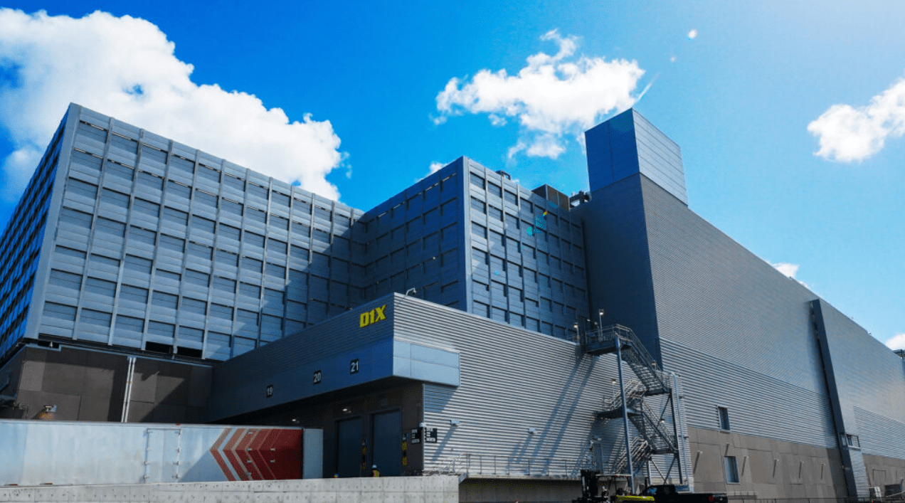
In September 2023, MSB2, a new support building for D1X, broke ground. This new facility will support logistics, equipment handling, and add 35,000 square feet of cleanroom space for D1X.
Intel's Fab 9 in Rio Rancho
Category | Details |
Fab Name | Intel Fab 9 |
Location | Rio Rancho, New Mexico, USA |
Owner | Intel Corporation |
Year Established | Originally 1987; reopened Jan 2024 |
Wafer Size | 300 mm (12-inch) |
Process Nodes | Advanced 3D packaging (Foveros & EMIB) |
Type of Fab | High-volume advanced 3D chip packaging |
Investment Cost | USD 3.5 billion |
Lithography | Not Disclosed |
Intel's Fab 9 was initially established in 1987; however, in January 2024, Intel reopened the facility after several expansions as part of a USD 3.5 billion investment. This facility serves Intel's 3D advanced packaging technologies, including Intel's Foveros 3D stacking and EMIB (Embedded Multi-Die Interconnect Bridge).
It is Intel's first high-volume US facility dedicated to advanced 3D chip packaging. Intel's Fab 9 works along with Fab 11X, ensuring end-to-end manufacturing from wafer production to advanced packaging.
Intel Ocotillo Campus
Category | Details |
Fab Name | Intel Fab 42 |
Location | Chandler, Arizona, USA |
Owner | Intel Corporation |
Year Established | 2020 |
Wafer Size | 300mm (12-inch) |
Process Nodes | 10nm, 7nm, Intel 4, Intel 3 |
Type of Fab | IDM |
Investment Cost | USD 50 billion (estimated) |
Lithography | EUV & DUV Lithography |
Intel’s Ocotillo campus, also known as Fab 42, produces 7 nm microprocessors that are used to power data centers and hundreds of millions of smart connected devices. It was established in 2020 by Intel Corporation with an estimated cost of USD 50 billion. The fab facility is located in Chandler, Arizona, USA.
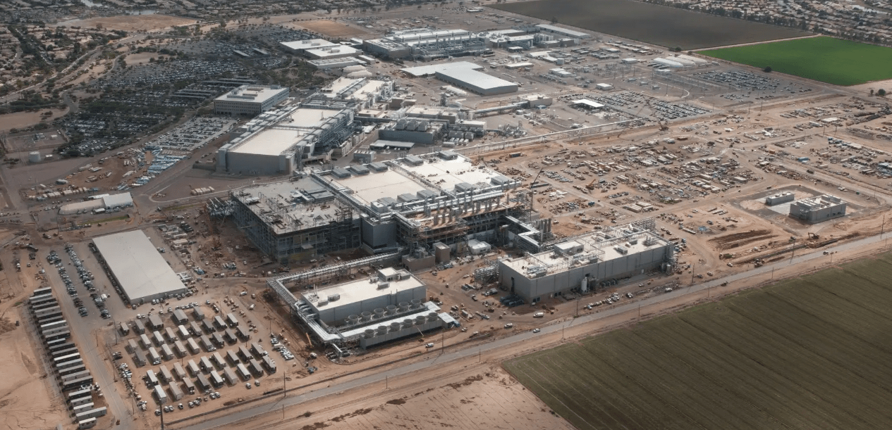
It produces chips on 300 nm (12-inch wafers) using EUV lithography for clients like Qualcomm, Nvidia, IBM, and more. Fab 52 and Fab 62 are under construction at Fab 42, which will help meet the growing demand for leading-edge chips for Intel foundry customers. Intel received up to USD 7.86 billion in direct funding from the U.S. Department of Commerce under the U.S. CHIPS and Science Act for this project.
Micron Boise Campus
Category | Details |
Fab Name | Micron Boise Campus |
Location | Boise, Idaho, USA |
Owner | Micron Technology |
Year Established | Broke ground Sep 2022; construction began Oct 2023 |
Wafer Size | 300 mm (12-inch) |
Process Nodes | Leading-edge DRAM & High Bandwidth Memory (HBM) |
Type of Fab | Memory fabrication plant (AI-focused HBM production) |
Investment Cost | USD 6.4 billion (CHIPS Act funding for Idaho & other fabs) |
Lithography | DUV Lithography |
The Micron Boise Campus is a memory fabrication plant also referred to as Boise fab. It is located in Boise, Idaho, United States, and is owned by Micron Technology. This project broke ground in September 2022, and construction began in October 2023.
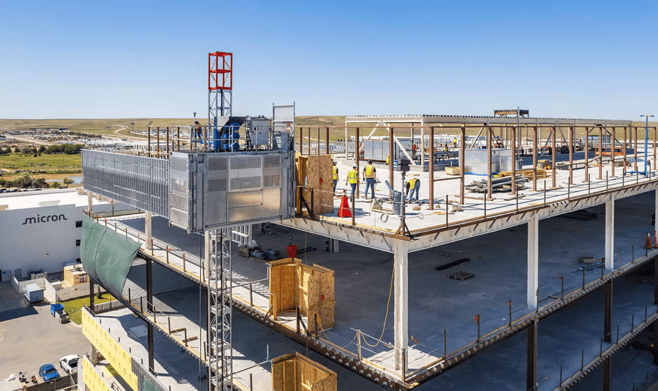
This new fab plant in Idaho, United States, will feature two leading-edge fabs, these two fabs will include High Bandwidth Memory (HBM) essential for the AI market. Micron has already secured USD 6.4 billion in funding under the CHIPS Act for the construction of two Idaho fabs and two New York fabs, along with expansion planned for its Virginia fab. The construction of the first Idaho fab with DRAM output is already completed and is expected to come online in 2027.
40+ reviews
Find the Latest Semiconductor Projects Across United States
Gain exclusive access to our industry-leading database of semiconductor project opportunities with detailed project timelines and stakeholder information.
Collect Your Free Leads Here!
No credit cardUp-to-date coverage
Joined by 750+ industry professionals last month
Samsung Austin Semiconductor
Category | Details |
Fab Name | Samsung Austin Semiconductor (S1 & S2) |
Location | Austin, Texas, USA |
Owner | Samsung Electronics |
Year Established | 1996 (S1); S2 came online 2007 |
Wafer Size | 300 mm (12-inch) |
Process Nodes | 14 nm to 65 nm (Logic & Memory) |
Type of Fab | Logic and memory semiconductor fabrication; NAND Flash production |
Investment Cost | USD 18 billion |
Lithography | DUV Lithography |
The Samsung Austin Semiconductor plant is an automated plant with a volume production of 300 nm fab plant in Austin, Texas. This plant specializes in Logic and memory chips with technology nodes from 14 nm to 65 nm. This site was built in 1996 and was modeled after the Hwaseong semiconductor site in Korea. It was built with an investment of USD 18 billion and includes two fabs it S1 and S2 fabs covering 2.76 million total square footage of floor space.
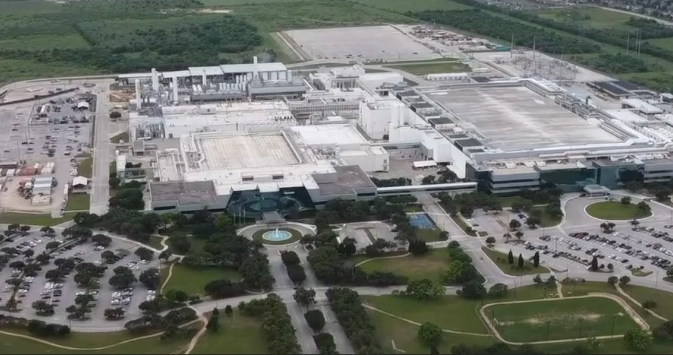
In March 1997, it began its first semiconductor fab in Austin, and in April 2006, it broke ground for a second fabrication unit to manage the increased product demands, which came online in June 2007. In December 2007, it began NAND Flash Technology production, and in August 2009, the fab plant converted to 300 nm process technology.
Taylor Semiconductor Plant
Category | Details |
Fab Name | Taylor Semiconductor Plant |
Location | Texas, USA |
Owner | Samsung Electronics |
Year Established | Broke ground in 2022; expected to be operational in 2026 |
Wafer Size | 300 mm (12-inch) |
Process Nodes | <16 nm / 14 nm (advanced nodes) |
Type of Fab | Advanced logic semiconductor fabrication (Smart Mobile, HPC, Automotive, IoT, Personal Computing) |
Investment Cost | USD 17 billion |
Lithography | EUV Lithography |
The Taylor Semiconductor plant is one of Samsung's largest-ever investments in the US. This plant is located in Texas, United States. It manufactures advanced nodes with less than 16 nm or 14 nm used in Smart Mobile Platforms, High-Performance Computing, Automotive Electronics Platform, Home and Industrial IoT Platform, and Personal Computing Platform.
Samsung built this plant with an investment of USD 17 billion. This cost includes buildings, property, improvements, machinery, and equipment. Samsung broke ground in 2022 and is expected to be operational by 2026.
Texas Instruments RFAB 1 & 2
Category | Details |
Fab Name | Texas Instruments RFAB 1 & 2 |
Location | Richardson, Texas, USA |
Owner | Texas Instruments |
Year Established | RFAB1: 2009; RFAB2: production started Sep 2022 |
Wafer Size | 300 mm (12-inch) |
Process Nodes | Analog chips on 300 mm wafers (mature node) |
Type of Fab | Analog semiconductor fabrication |
Investment Cost | Not Disclosed |
Lithography | DUV Lithography |
RFAB 1 & 2 are 300 nm wafer fabs by Texas Instruments located in Richardson, Texas. The RFAB1 became operational in 2009 and is known as the world's first 300 nm analog wafer fab. The RFAB2 broke ground in 2020 and began its initial production in September 2022. In 2023, RFAB2 achieved LEED Gold v4 certification. With a clean room space of approximately 650,000 square feet, Richardson 300 nm fabs together will manufacture more than 100 million analog chips per day.
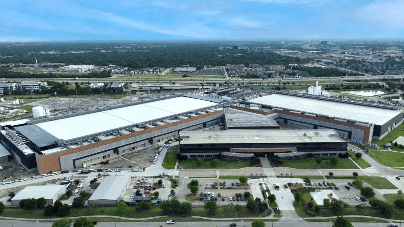
On 18th June 2025, Texas Instruments company announced its plans to invest USD 60 billion across seven US semiconductor fabs in Texas and Utah. One of these is the "largest mega-site" in Sherman, Texas, that will include four fabs, SM1, SM2, which are under way and two additional fabs, SM3, SM4, totalling the investment to USD 40 billion.
TSMC Arizona Fab 21
Category | Details |
Fab Name | TSMC Arizona Fab 21 |
Location | Phoenix, Arizona, USA |
Owner | TSMC |
Year Established | Construction began April 2021; 4 nm production started Q4 2024 |
Wafer Size | 300 mm (12-inch) |
Process Nodes | 2 nm to 5 nm (FinFET & nanosheet technology) |
Type of Fab | Leading-edge logic semiconductor fabrication (5G/6G, HPC, AI applications) |
Investment Cost | N/A (not specified in your text) |
Lithography | EUV Lithography |
The TSMC Fab 21, also known as TSMC Arizona, is one of the major TSMC fabs in the US, located in Phoenix, Arizona. This fab plant has three fab plants that collectively manufacture leading-edge logic chips used in 5G/6G smartphones, high performance computing, and AI applications.
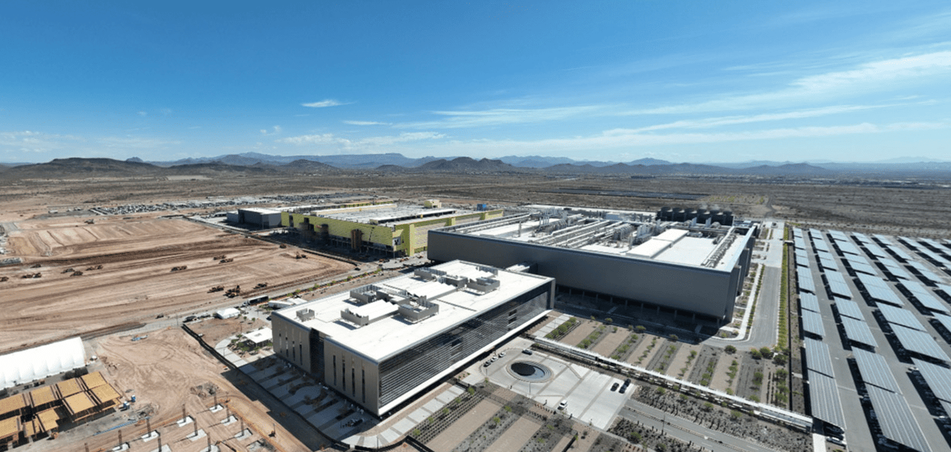
The first fab plant in phase 1 manufactures 4 nm and 5 nm FinFET process technology chips. The construction began in April 2021, and production of 4 nm process technology began in Q4 of 2024. With a production capacity of 10,000 wafers per month, it will reach its full capacity of 20,000 wafers per month by mid-2026. The two other fabs are Fab 2 and Fab 3, which will produce 3nm FinFEt and A16, 2 nm nanosheet process technologies, which are expected to enter volume production in 2028.
Conclusion
Semiconductor fabs in the United States continue to strengthen their position as a global semiconductor market leader, driven by key players like Intel, Samsung, TSMC, and GlobalFoundries.
These fabs are advancing in technologies through frequent expansions, meeting the growing demand. As semiconductor demand grows from AI and cloud computing to automotive and consumer electronics, new semiconductor fab plants and cutting-edge technological advancements become essential to maintain supply-demand chain sustainability and secure the US position in the global semiconductor market.
Stay Ahead with the Latest Semiconductor Fab Projects!
Subscribe to Blackridge’s US Semiconductor Fab Plants Database and gain exclusive access to:
Reliable, high-quality insights on the semiconductor industry
Comprehensive project tracking – upcoming, in-progress, and completed fabs
Key EPC projects & material suppliers, stakeholder details for strategic decision-making
Timely updates to keep you informed and ahead of the competition
Start your free demo today and power your business with data-driven success!
Leave a Comment
We love hearing from our readers and value your feedback. If you have any questions or comments about our content, feel free to leave a comment below.
We read every comment and do our best to respond to them all.