
Table of Contents
Semiconductors are driving the digital economy and are widely used across automobiles, electronics, data storage, wireless communication, and artificial intelligence. Largest semiconductor fabs like TSMC fab 18, Samsung Pyeongtaek campus, and many more are thriving to meet the increasing global semiconductor demand. According to the Semiconductor Industry Association (SIA), global semiconductor sales hit USD 56.55 billion in January 2025, which is a 17.9% increase compared to January 2024.
Furthermore, with Taiwan as a major player in the semiconductor industry, countries like India, the U.S., Japan, and South Korea are hugely investing in new semiconductor plants, expanding their market share.
In this blog, we will explore some of the world’s most significant semiconductor fabrication plants and also a few of the major upcoming semiconductor fab plant projects by industry giants like TSMC, Micron Technologies, SK Hynix, and Semiconductor Manufacturing International Corporation (SMIC). Keep reading to know more!
List of Largest Semiconductor Fabs in the World
TSMC Fab 18
Category | Details |
Fab Name | TSMC Fab 18 |
Location | Tainan, Taiwan |
Owner | Taiwan Semiconductor Manufacturing Company |
Year Established | 2020 |
Wafer Size | 12-inch (300mm) |
Process Nodes | 5nm, 3nm |
Type of Fab | Pure-play Foundry |
Investment Cost | USD 15.24 billion |
Key Clients | Apple, AMD, Qualcomm, Nvidia |
Lithography | EUV Lithography |
TSMC’s Fab 18 is its fourth 12-inch GigaFab® in Taiwan after Fab 12, Fab 14, and Fab 15. It specializes in producing 5nm and 3nm (nanometer) process node technology. Fab 18 is constructed at an estimated cost of NT$500 billion.
The groundbreaking ceremony was held on 26 January 2018. It was built in multiple phases. Phase 1 construction was completed by Q1 of 2019. Phase 2 construction began in Q3 of 2018, and Phase 3 construction began in Q3 of 2019. The first two phases entered production by 2020, while phase 3 entered production by 2021.
It is located in the Southern Taiwan Science Park and is TSMC's largest semiconductor fab plant owned by TSMC Nanjing Company Limited. It is built across 42 hectares, with a floor area of 950,000 square meters and a total cleanroom area of 160,000 square meters, which is equal to 25 standard soccer fields.
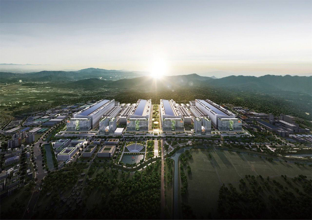
Samsung Pyeongtaek Campus
Category | Details |
Fab Name | Samsung Pyeongtaek Campus |
Location | Pyeongtaek, Gyeonggi Province, South Korea |
Owner | Samsung Electronics |
Year Established | 2015 (First fab started operations in 2017) |
Wafer Size | 300mm (12-inch) |
Process Nodes | 3nm, 4nm, 5nm, 7nm, 14nm, DRAM |
Type of Fab | IDM (Integrated Design Manufacturers) |
Investment Cost | |
Key Clients | Qualcomm, NVIDIA, IBM, Baidu |
Lithography | EUV & DUV Lithography |
The Samsung Pyeongtaek semiconductor fabrication plant has three facilities: P1, P2, and P3. The P1 line focuses on the production of Samsung's fourth-generation V-NAND (64 layers). When it broke ground in May 2015, it was the largest single fab in the industry.
The P2 facility is near the P1 line in the Godeok Industrial Complex in Pyeongtaek Campus. The production line covers a gross area of 128,999 square meters and focuses on the production of third-generation 10 nm mobile DRAM using the EUV process, V-NAND, and ultra-micro foundries. P2 entered production in 2020.
The P3 facility, which entered production in July 2022, produces DRAM products with a 14 nm process and additionally offers 5nm or advanced nodes for its clients.
Intel Fab 42
Category | Details |
Fab Name | Intel Fab 42 |
Location | Chandler, Arizona, USA |
Owner | Intel Corporation |
Year Established | 2020 |
Wafer Size | 300mm (12-inch) |
Process Nodes | 10nm, 7nm, Intel 4, Intel 3 |
Type of Fab | IDM |
Investment Cost | USD 50 billion (estimated) |
Key Clients | Qualcomm, Nvidia, and IBM, Dell, HP, Lenovo |
Lithography | EUV & DUV Lithography |
Intel’s Fab 42 is a semiconductor fab plant in Chandler, Arizona, also known as the Ocotillo fab plant. The plant produces 7 nm microprocessors used to power data centers and hundreds of millions of smart and connected devices.
Fab 52 and Fab 62 are under construction at Fab 42, which will help meet the growing demand for leading-edge chips for Intel foundry customers. Intel received up to USD 7.86 billion in direct funding from the U.S. Department of Commerce under the U.S. CHIPS and Science Act for this project. The total project cost for Fab 42 is estimated to be about USD 50 billion.
Global Foundries Fab 8
Category | Details |
Fab Name | GlobalFoundries Fab 8 |
Location | Malta, New York, USA |
Owner | GlobalFoundries |
Year Established | NA |
Wafer Size | 12-inch (300mm) |
Process Nodes | 12nm, 14nm, 40 nm |
Type of Fab | Pure-play Foundry |
Investment Cost | Over USD 15 billion |
Key Clients | U.S. Department of Defence |
Lithography | DUV Lithography |
GlobalFoundries Fab 8 is one of the largest semiconductor fab plants located in Malta, New York. It entered production in 2009. The GlobalFoundries (GF) fab 8 plant produces 12 nm chips and above for FinFET devices on 300 mm wafers (12-inch wafers). The Fab 8 plant was built at a cost of more than USD 15 billion by GlobalFoundries. Fab 8 has a current capacity of 400,000 wafers per year.
GlobalFoundries Inc. signed a USD 117 million agreement with the U.S. Department of Defence (DoD) to provide a strategic supply of US-made semiconductors from the Fab 8 Malta facility that will be used in the US's most sensitive defense and aerospace applications. Earlier these chips were supplied from GF's Fab 10 in East Fishkill, New York. Fab 8 produces chips for the country's defense and also offers a 45nm SOI platform for commercial customers.
The Fab 8 plant is undergoing expansion and will establish a new 358,000-square-foot manufacturing facility at the Malta campus. Governor Kath Hochul announced on February 19, 2024, that Saratoga County-based GlobalFoundries will invest USD 11.6 billion in the next 10 years in the Fab 8 semiconductor fab plant in New York. This expansion is expected to triple the plant's existing capacity.
The expansion is expected to begin in 2025, this expansion of production of mature nodes is supported by USD 575 million funded by performance-based Green CHIPS tax credits in expansion to create about 11,508 direct jobs at the site.
GlobalFoundries will also receive USD 30 million in infrastructure investment from the state's New York Power Authority.
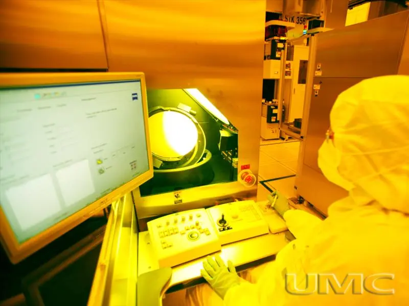
UMC Fab 12A
Category | Details |
Fab Name | UMC Fab 12A |
Location | Tainan Science Park, Taiwan |
Owner | United Microelectronics Corporation (UMC) |
Year Established | 2002 |
Wafer Size | 300mm (12-inch) |
Process Nodes | 14nm, 22nm, 28nm, 40nm, and 55nm |
Type of Fab | Pure-play Foundry |
Investment Cost | Over 8 billion |
Key Clients | Qualcomm, MediaTek, Broadcom, Texas Instruments, Realtek |
Lithography | DUV Lithography |
United Microelectronics Corporation (UMC) fab 12A is one of the UMC's largest production and research & development sites. Located in Tainan Science Park, Tainan, Taiwan, it entered volume production in 2002 and manufactures products 14nm, 22nm, 28nm, 40nm.
The Fab 12A was Taiwan's first 300mm (12 inch) fab plant from phases 1-4. This facility had phases 1-6 and currently manufactures customer products using 28nm High-K/Metal gate and 14nm FinFET technologies. The Fab 12's phase 1-4 projected USD 8 billion, with P5&P6 projected USD 8 billion.
Fab 12's phases 5&6 was planned to extend the plant capacity to produce 28 nm and 20 nm to meet customer demand. UMC announced its plans to expand the plant further to P7 & P8. With P5 & P6 expansion producing 50,000 wafers per month, Fab 12 A's total monthly design capacity has reached 130,000 wafers.
In 2023, UMC announced its plans to expand Fab 12A phase 6 (P6) through a collaboration model with several leading global customers.
On 14th January 2025, UMC's flagship project, 12A in Tainan, was selected for the World Economic Forum's Global Lighthouse Network. It is the first semiconductor foundry globally to earn Lighthouse status. Lighthouses are manufacturing plants designated by a panel of experts based on their effective use of AI, industrial Internet of Things (IIoT), big data analytics, and other digital technologies. The Global Lighthouse Network was co-founded by World Economic Forum and McKinsey & Company in 2018.
Taylor Semiconductor Plant
Category | Details |
Fab Name | Taylor Semiconductor Plant |
Location | Texas, United States |
Owner | Samsung Electronics |
Year Established | Expected operational by 2026 |
Wafer Size | Not publicly disclosed |
Process Nodes | Advanced node (less than 16 nm or 14 nm) |
Type of Fab | Advanced Semiconductor Fabrication Plant |
Investment Cost | USD 17 billion |
Key Clients | Qualcomm, NVIDIA, IBM, Baidu |
Lithography | EUV lithography |
Taylor Semiconductor plant, located in Texas, United States is one of Samsung's largest-ever investments in the US. This plant is an advanced node plant (less than 16 nm or 14 nm). The chips produced in this plant will be used in Smart Mobile Platforms, High-Performance Computing/Datacenter Platform, Automotive Electronics Platform, Home and Industrial IoT Platform, and Personal Computing Platform.
Samsung invested about USD 17 billion in this project which includes buildings, property, improvements, machinery, and equipment. Samsung broke ground in 2022 and is expected to be operational by 2026.
Also Read: Taylor Semiconductor Manufacturing Plant
Yongin Plant
Category | Details |
Fab Name | Yongin Cluster |
Location | Wonsam-myeon, Yongin, Gyeonggi Province, South Korea |
Owner | SK Hynix |
Year Established | First fab: May 2027. Targeted completion: 2036. |
Wafer Size | 300mm |
Process Nodes | 16nm, 14nm |
Type of Fab | DRAM, HBM |
Investment Cost | KRW 122 trillion |
Lithography | EUV lithography |
Status | Planning |
SK Hynix announced its plans to build four fabs at the Yongin cluster. The Yongin cluster is expected to be made operational by 2036 with all four fabs. The entire Yongin cluster is planned over an area of 4.15 million square meters with a project cost of KRW 122 trillion (USD 85.5 billion). It is planned in Wonsam-Myeon, Yongin, Gyeonggi Province.
On 26th July 2024, SK Hynix approved the investment plan for the first fab of the Yongin cluster with a project cost of 9.4 trillion won (USD 6.48 billion). The construction is expected to begin in March 2025 and is expected to begin volume production by May 2027. The first fab will produce DRAMS, including HBM. SK Hynix also plans to build a "Mini-fab2) within fab 1 to help small businesses develop, demonstrate, and evaluate technologies.
The investment period planned for the Yongin plant is from August 2024 to the end of 2028. On 26th December 2024, the government of South Korea designated the Yongin complex as the National Industrial Complex due to its location and multiple fab plants situated in the location.
40+ reviews
Find the Latest Upcoming Semiconductor Projects Around the World
Gain exclusive access to our industry-leading database of semiconductor project opportunities with detailed project timelines and stakeholder information.
Collect Your Free Leads Here!
No credit cardUp-to-date coverage
Joined by 750+ industry professionals last month
Upcoming Semiconductor Fab Plants
Tata Electronics New Semiconductor fab plants in Gujarat
Tata Electronics plans to develop two semiconductor fab plants in Dholera, Gujarat. The first fab plant is planned in the Dholera Special Investment Region in Gujarat. Tata Electronics broke ground in March 2024, and it is expected to enter production by 2026.
This semiconductor plant in Dholera phase 1 is planned with a cost of INR 91,000 crores (USD 10.44 billion) that will produce about 50,000 wafers per month. It will produce power production circuits, display drivers, microcontrollers, and high-performance computing logic chips that will be used in automotive, data storage, wireless communication, artificial intelligence, and more.
It is being developed in partnership with Taiwan's Powerchip Semiconductor Manufacturing Corporation (PSMC). The second and third semiconductor fabs are also being planned, which will enter construction within the next five to seven years.
On 6th March 2025, Tata Electronics signed a MoU worth USD 11 billion for the Dholera semiconductor fab plant. The Dholera plant is set to become India's biggest foundry. It is Tata Electronics' second largest investment after its investment of INR 27,000 crores (USD 3.10 billion) in Assam's semiconductor assembly and testing facility.
Also Read: Top Upcoming Semiconductor Projects in India
TSMC Arizona
TSMC Arizona which began high-volume production of N4 process technology in the Q4 of 2024, is set for expansion with a second fab in the site that will lead edge N3 process technology and that will be operational by 2028. A third fab is also being planned at the sit,e which will manufacture chips using 2nm or even more advanced process node technology, which is expected to be operational by 2030.
On 4th March 2025, TSMC announced its plans for a USD 100 billion investment in collaboration with the US government under the presidency of Donald Trump. This investment will support the building of five additional semiconductor chip facilities in the country. As a part of the investment, TSMC announced its plans to build three new semiconductor fabrication facilities, two advanced packaging facilities, and a major R&D center in the country.
TSMC plants in Kumamoto, Japan
On 25th February 2024, Japan announced its USD 4.9 billion investment to TSMC for building a second chip fabrication plant in Japan. TSMC, on 24th February 2024, opened its first Japan chip plant in Kumamoto. This factory currently produces logic chips with 12 to 28 nm process technologies that will be used in cars, and image sensors for its client Sony Group Corp. and auto parts maker Denso Corp.
This second chip plant is expected to offer a capacity of more than 100,000 12-inch wafers per month, which is expected to be operational by 2027. These two plants together are expected to create more than 3,400 high-tech professional jobs.
40+ reviews
Find the Latest Upcoming Semiconductor Projects Around the World
Gain exclusive access to our industry-leading database of semiconductor project opportunities with detailed project timelines and stakeholder information.
Collect Your Free Leads Here!
No credit cardUp-to-date coverage
Joined by 750+ industry professionals last month
Sanad semiconductor plant, Micron Technologies
Tata Projects is building the semiconductor assembly and test facility in Sanad, Ahmedabad, India for Micron Technology. The plant is being built across 50 acres of land at a cost of USD 2.7 billion. The Micron Technology Plant in Sanand will include assembly, Testing, Marketing, and Packaging (ATMP) facilities. In June 2023, the Gujarat government signed a Memorandum of Understanding with Micron Technologies for the plant.
On 28th January 2025, Tata Projects announced about 60% of Phase 1 has been completed by India's first semiconductor plant. The civil work, mechanical, electrical, and plumbing work are to be completed and handed over to Micron by December 2025.
Mega-Fab Plant in Clay, Micron Technologies
In October 2022, Micron Technologies announced megafab plant in Clay, New York. This facility is part of Micron’s USD 100 billion investment plan, marking the largest semiconductor manufacturing investment in U.S. history. The plant will include four 60,000 square-foot cleanrooms of a total of 2.4 million square feet clean room space equal to 40 U.S. football fields.
On 18th April 2024, Micron Technologies secured USD 6.1 billion in funds through a preliminary agreement for its mega-fab plant in Clay. These funds are awarded under the CHIPS & Science Act. This mega fab plant is expected to be completed within 2 decades with a total estimated cost of USD 100 billion, creating about 50,000 jobs in the Central New York region.
Texas Instruments LFAB2
On 2nd November 2023, Texas Instruments broke ground for a semiconductor plant in Utah. This 300 mm semiconductor wafer fabrication plant is named LFAB2 and is located near the company's existing LFAB1 plant in Lehi, Utah. This plant, along with LFAB1, will manufacture millions of analog and embedded processing chips. LFAB2 in Utah is being built with an investment of USD 11 billion and is expected to enter production by 2026.
Conclusion
The semiconductor industry is witnessing immense growth through large semiconductor companies such as Taiwan Semiconductor Manufacturing Co (TSMC), Samsung Electronics, Intel Corporation, and SK Hynix, the leading chip manufacturing industry. Countries like Taiwan, the United States, South Korea, and India are witnessing expansion in the semiconductor industry through plans rolled out for new and advanced semiconductor fab plants that will bridge the growing demand and supply gap through advanced process node technology chips that are used in AI, data centers, automobiles, and consumer electronics.
Advancements in memory chips and advanced micro devices are challenging innovations in semiconductor manufacturing. As technology evolves, the semiconductor industry continues to grow and expand.
FAQ'S
Which is the largest semiconductor fab in the world?
Taiwan Semiconductor Manufacturing Company (TSMC) is known as the world's largest semiconductor fab, operating multiple gigafab including FAB 18 in Taiwan, which is one of the largest and most advanced semiconductor fabs.
How much is the cost of a semiconductor fab?
The estimated cost of semiconductor fab plant construction ranges from USD 10 billion to USD 20 billion.
Is TSMC a fab or foundry?
TSMC (Taiwan Semiconductor Manufacturing Company) is a dedicated IC Foundry business model founded in 1987.
Are there any semiconductor fabs in India?
India has new semiconductor fab plants developed in Dholera, Gujarat with a capacity of 50,000 wafers per month. It has other semiconductor assembly and testing facilities by Micron Technologies in Sanand and Tata Electronics in Assam.
Stay Ahead with the Latest Semiconductor Fab Projects!
Subscribe to Blackridge’s Global Semiconductor Fab Plants Database and gain exclusive access to:
Reliable, high-quality insights on the semiconductor industry
Comprehensive project tracking – upcoming, in-progress, and completed fabs
Key EPC projects & stakeholder details for strategic decision-making
Timely updates to keep you informed and ahead of the competition
Start your free demo today and power your business with data-driven success!


Leave a Comment
We love hearing from our readers and value your feedback. If you have any questions or comments about our content, feel free to leave a comment below.
We read every comment and do our best to respond to them all.