Call +1(917) 993 7467 or connect with one of our experts to get full access to the most comprehensive and verified construction projects happening in your area. 

Last Updated on 23
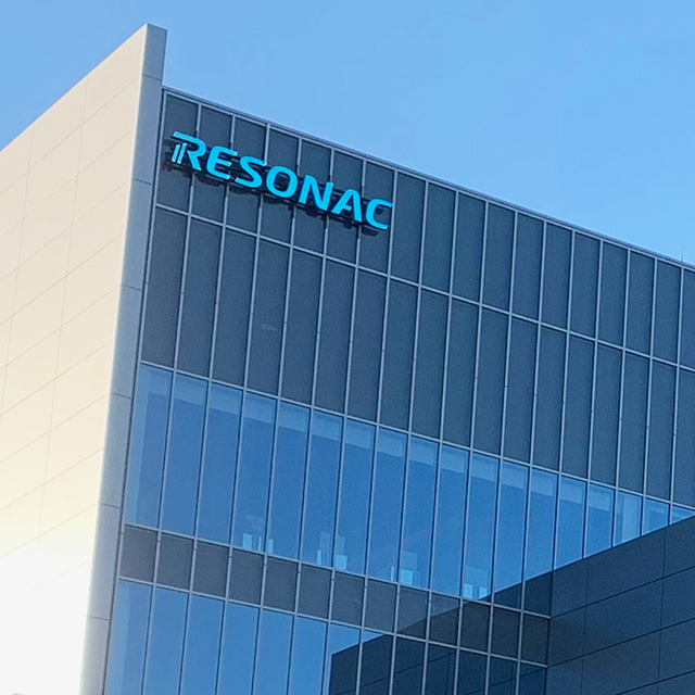
Japanese chip manufacturer Resonac, in a press release, stated that it will set up a research and development center for advanced semiconductor packaging and materials in Silicon Valley, USA. Resonac has already started scouting facilities to develop its packaging facility center. The facility is expected to start its operations by 2025.

Resonac has started preparations to establish a new PSC (Packaging Solutions Center), which is a research and development center for advanced semiconductor packaging materials technologies, in Silicon Valley. The new R&D center will be equipped with state-of-the-art facilities for research and development in semiconductor packaging and materials. The center will also have a clean room and equipment for manufacturing semiconductor materials.
Resonac established its first PSC in Shin Kawasaki, Japan. This facility can process large-sized materials such as 300mm semiconductor wafers and a 500mm square panel. These facilities are capable of laser dicing, fine wiring formation, and handling processes and materials for semiconductor packaging.
The global Semiconductor market is projected to exceed USD 1 trillion by 2030. The establishment of the new R&D center is a positive development for the semiconductor industry in the United States. The center will help foster innovation and collaboration in the industry and will help ensure that the United States remains a leader in semiconductor manufacturing. Earlier this week, the US unveiled its USD 3 billion vision for the National Advanced Packaging Manufacturing Program.
Resonac Corporation is a Japanese multinational company that specializes in developing and manufacturing advanced materials for a wide range of industries, including electronics, energy, and environment. Founded in 1936, Resonac has a long history of innovation and is recognized as a leading supplier of high-performance materials.
Resonac has a global presence with manufacturing facilities and sales offices in over 20 countries. The company is committed to innovation and sustainability, and it is constantly developing new products and technologies to meet the needs of its customers.
Are you looking for a platform that gives you reliable, high-quality, and timely project insights for Semiconductor Manufacturing Projects in the United States?
Discover the Global Project Tracking (GPT) platform by Blackridge Research, designed to provide you with the most recent United States Semiconductor Fabrication Plant Projects and Tenders better and faster across various stages of development:
The user-friendly interface helps you obtain early-stage awareness of projects and find the right business opportunity quickly.
Each project will have all the essential details, such as scope, capacity, CapEx, status, project description, companies involved, funding information, location, periodic updates, important event dates like construction start date, commissioning dates, and key contact information of project owners and stakeholders.
The database is a vital resource for a wide range of entities, including semiconductor manufacturers, EPC Companies, silicon material suppliers, data analytics and software providers, consulting and advisory firms, investors, multilateral banks and financial institutions, and law firms.
Book a Free demo to learn more about the United States Semiconductor Fab Projects and Tenders database and how we can help you achieve your goals.

News_Release 10th Nov 2023

News_Release 20th Nov 2023

News_Release 21st Nov 2023
News_Release 23rd Nov 2023

News_Release 23rd Nov 2023

News_Release 28th Nov 2023
